Download
1 / 20
220 likes | 481 Vues
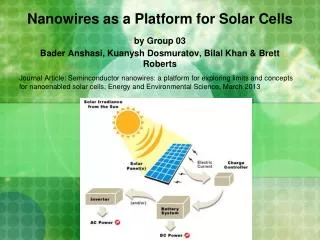
Journal Article: Seminconductor nanowires: a platform for exploring limits and concepts for nanoenabled solar cells, Energy and Environmental Science, March 2013. Nanowires as a Platform for Solar Cells. by Group 03 Bader Anshasi, Kuanysh Dosmuratov, Bilal Khan & Brett Roberts. Abstract.

E N D
Journal Article: Seminconductor nanowires: a platform for exploring limits and concepts for nanoenabled solar cells, Energy and Environmental Science, March 2013 Nanowires as a Platform for Solar Cells by Group 03 Bader Anshasi, Kuanysh Dosmuratov, Bilal Khan & Brett Roberts
Abstract Basic Layout of a traditional Silicon Solar Cell https://spie.org/Images/Graphics/Newsroom/Imported-2010/002654/002654_10_fig1.jpg Nanowire Solar Cell To improve the performance of traditional silicon-based solar cells. On the right is the basic layout of a nanowire solar cell. http://large.stanford.edu/courses/2012/ph241/kumar2/images/f1big.png
What are solar cells? • Photovoltaic effect:Electricity is generated by means of absorption of light by electrons in the valence band of a semiconductor. Silicon Solar Cell. How Solar Cells Work • "A solar cell (also called a photovoltaic cell) is an electrical device that converts the energy of light directly into electricity by the photovoltaic effect." • Figures from: http://en.wikipedia.org/wiki/Solar_cell http://upload.wikimedia.org/wikipedia/commons/4/48/PnJunction-PV-E.PNG http://www.solarbotics.net/starting/200202_solar_cells/pix/solar2.gif
Problems faced with current solar cell technology Different kinds of solar cells Low efficiencies are caused by: incomplete light absorption, carrier recombination and thermal losses. • Monocrystalline: made of single crystalline silicon of high purity. Figure A Polycrystalline:, made up polycrystalline silicon Figure B Figure from: http://sroeco.com/solar/solar-panel-efficiency-tiers Figure A: http://upload.wikimedia.org/wikipedia/commons/0/04/125x125-pseudo-square-monocrystalline-solar.cell.jpg Figure B: http://www.solar-energy-at home.com/images/polycrystalline_photovoltaic_cell.jpg Figure C: http://www.sunconnect.com.au/wpcontent/uploads/2011/08/aaa5.jpg Thin film:Made of several thin layers of semiconductor material. Figure C
Nanowires to the rescue • Use Nanowires! • Very small, increases surface area for light absorption • Great potential http://consciouslifenews.com/wp-content/uploads/2013/01/nanowires_hairy_solar_cell.jpg • Nanowires in solar cells • Increased efficiency http://spie.org/Images/Graphics/Newsroom/Imported/1087/1087_fig1.jpg
Synthesis of Nanowires (1) A bottom up approach: method used to synthesize nanowires in this article is by a vapor-liquid-solid (VLS) growth process. This process is shown below below: • Control of: • Geometry • Material • Structure and morphology. VLS growth cycle Nucleation Nanowire formation Figure by: H J Choi, Vapor-Liquid-Solid Growth of Semiconductors, Chap. 1
Synthesis of Nanowires (2) • Laser interference lithography and metal assisted etching. • Capable of producing nanowires with diameters between 50 - 300 nm. • Allows for the production of ordered and periodic nano structures. As shown below. The figure above shows silicon nanowires that exhibit both order and bunching. Both Figures by: J Boor and V Schmidt, Nanowires by laser interference lithography and metal-assisted etching , 2007. Fabrication process
Control of Geometry • Nanowire devices are synthesized into p-i-n (p-type/intrinsic/n-type) • junctions to achieve charge separation. Two geometries have been • investigated Axial Geometry It was found that axial is more efficient than radial. • Pink: p-type • Yellow: intrinsic • Blue: n-type Radial Geometry Figure from: Energy & Environmental Science, Vol. 6, Num. 3, pg 719-733.
Control of Material • Nanowires have been made of many different elements that have semiconductor properties including elements from group IV, III/V and II/VI. • Different combinations have different photovoltaic properties • Need to determine which one has the greatest efficiency Bright-field TEM images of this nanowire with an energy dispersive x-ray spectroscopy map. • For Example • Radial geometry • Germanium core- Red • Silicon Shell- Blue Figure from: Energy & Environmental Science, Vol. 6, Num. 3, pg 719-733.
Control of Morphology • Morphology affects light absorptoin properties of nanowires • Possible morphologies: At T=775 oC produced gives a hexagonal cross section At T=860 oC, cross section became more rectangular Hexagonal Figure on the right shows SEM images of nanowire building blocks. Figure above shows cross section of a hexagonal and rectangular nanowires. Octagonal Rectangular • Figure from: Energy & Environmental Science, Vol. 6, Num. 3, pg 719-733.
Current/Voltage Characteristics • Geometry optimization has led to a max Voc (open circuit voltage) of 0.48 V, the highest observed in a nanowire to date. • Similarly, the optimized core multi-shell geometry also yielded a Jsc (short circuit current density) between 8-10 mA/cm-2, much higher than expected. • Using different types of metal catalysts for the etching process has a direct effect on the Current-Voltage (I-V) relationship in NW devices I-V curves in an Si core. The grey and red curves correspond to Al catalyst and Au catalyst used for etching respectively. Open circuit voltage versus logarithm of ratio of short-circuit current (Isc) to dark saturation current (Io) • Figure sfrom: Energy & Environmental Science, Vol. 6, Num. 3, pg 719-733.
Light Absorption in Nanowires: Basic Theory • To increase electrical performance, solar cells must absorb a significant amount of light. • Maximizing the light absorption efficiency of NW is done finding the best material, size (diameter) and cross sectional morphology. • EQE (external quantum efficiency): used as a measure of efficiency for absorption of light by nanowires. Greater EQE means more efficient absorption. Figure from: http://en.wikipedia.org/wiki/External_quantum_efficiency
Light Absorption in Nanowires: Basic Theory • EQE varies with wavelength and at certain wavelengths there are resonance peaks where EQE>1 • Absorption efficieny varies with wavelength of incident light. Absolute EQE versus wavelength of incident light for a p-i-n core/multishell NW device. Absorption spectrum for a Ge NW • Figures from: Energy & Environmental Science, Vol. 6, Num. 3, pg 719-733.
Light Absorption: size Observations: • 1. Diameter Number of peaks • 2. Identical absorption modes shift to longer wavelengths with increasing NW diameter. Diameter: 170 nm Diameter: 280 nm Figure from: Energy & Environmental Science, Vol. 6, Num. 3, pg 681-1048 • For best efficiency, try to tune the absorption peaks so that they correspond to the wavelength of light that is most intense in the solar spectrum. • Greater diameter increases photocurrent perunit area • Greater diameter decreasesphotocurrent perunit volume. Diameter: 380 nm Figure from: Energy & Environmental Science, Vol. 6, Num. 3, pg 719-733.
Light Absorption: Morphology • Figure C shows how morphology affects photocurrent density. Cross sectional shape has a great effect on current. • Figure D shows that the peaks for absorption efficiency are shifted between 650 and 800 nm for the different kinds of morphologies . Figures from: Energy & Environmental Science, Vol. 6, Num. 3, pg 719-733.
Light Absorption: Morphology • Figure:comparison of the EQE spectra of a rectangular and hexagonal cross section of equivalent size. • Peaks centered at 565 nm and 680 nm are observed for both cross sections, rectangular one shows a much greater amplitude. • Choosing a certain morphology can improve light absorption properties of NWs Figures from: Energy & Environmental Science, Vol. 6, Num. 3, pg 719-733.
Assembly and scaling of nanowires for photovoltaic applications • Performance of a solar cell is often measured by factors of Jsc, Voc, and Isc. The current density, Jsc, is seen in figure (A) as increasing with the number of NW in a parallel array. • The efficiency of vertically stacked core-shell NW on a quartz substrate are predicted at around 15% or greater. • A layered stack of 5 NW without a backsidereflector can yield Jsc around 24 mAcm-2 and adding a backside reflector can increase this value to >40 mAcm-2 A - Current and current density as a function of the # of NW in parallel array. B - Current density increasing with more predictability in array vs. single NW. C - Comparing enhanced Jsc with absolute Jsc (right). D - EQE spectra. E - Current increasing with the number of NW in a vertical stack. Figure from: Energy & Environmental Science, Vol. 6, Num. 3, pg 719-733.
Figures (A), (B), and (C) show how a multi-junction solar cell can be made from stacking nanowires. This offers an aspect of versatility and control not seen in their crystalline silicon counterparts. NW size, morphology, and material composition can be tuned independent of the assembly of the solar cell. Figure from: Energy & Environmental Science, Vol. 6, Num. 3, pg 681-1048.
Conclusions • Use of nanowires as a module for solar cell production can potentially offer greater efficiencies and lowers costs. • With synthesis methods such as VLS and laser interference lithography, it is possible to very accurately control nanowire architecture including: size, morphology and material. • Voc (open circuit voltage) can be increased greatly by varying architecture. • Increasing the diameter will increase the absoprtion efficiency of nanowires. • A rectangular cross section nanowire has the greatest absorption efficiency • Nanowire manufacturing can be scaled up and assembled into arrays to produce the solar cells. An array of Si nanowires Figure from: http://consciouslifenews.com/nanowires-make-powerful-solar-cells/1147974/
Follow Up Analysis • Moving ahead, there are three key areas in nanowire research that can be further developed. These include: 1) Synthesis of nanomaterial with improved photovoltaic properties. 2) Large scale plans for assembly and production of photovoltaic nanowires. 3) Explore power-generating photovoltaic nanowires • This nanowire photovoltaic device research can also be used for other applications. For example, a photovoltaic nanomaterial is essentially a self-powered system. It could be used to embed nanosensors within the human body for monitoring health. Nanosensor used to monitor cellular interaction in a human body. Figure from: http://www.topnews.in/researchers-develop-nanosensor-monitors-cellular-interactions-realtime-2335464/