Multiplier Example
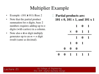
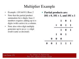
Multiplier Example. Partial products are: 101 x 0, 101 x 1, and 101 x 1. Example: (101 x 011) Base 2 Note that the partial product summation for n digits, base 2 numbers requires adding up to n digits (with carries) in a column.

Multiplier Example
E N D
Presentation Transcript
Multiplier Example • Partial products are: 101 x 0, 101 x 1, and 101 x 1 • Example: (101 x 011) Base 2 • Note that the partial productsummation for n digits, base 2 numbers requires adding up to n digits (with carries) in a column. • Note also nx m digit multiplygenerates up to an m + n digitresult (same as decimal). KU College of Engineering Elec 204: Digital Systems Design
Example (1 0 1) x (0 1 1) Again • Reorganizing example to follow hardware algorithm: Clear C || A Multipler0 = 1 => Add B Addition Shift Right (Zero-fill C) Multipler1 = 1 => Add B Addition Shift Right Multipler2 = 0 => No Add, Shift Right KU College of Engineering Elec 204: Digital Systems Design
Multiplier Example: Block Diagram IN n -1 n Multiplicand Counter P Register B n log n 2 Zero detect G (Go) Parallel adder C out Z n n Multiplier Q Control o unit 0 C Shift register A Shift register Q 4 n Product Control signals OUT KU College of Engineering Elec 204: Digital Systems Design
Multiplexer Example: Operation • The multiplicand (top operand) is loaded into register B. • The multiplier (bottom operand) is loaded into register Q. • Register C|| A is initialized to 0 when G becomes 1. • The partial products are formed in register C||A||Q. • Each multiplier bit, beginning with the LSB, is processed (if bit is 1, use adder to add B to partial product; if bit is 0, do nothing) • C||A||Q is shifted right using the shift register • Partial product bits fill vacant locations in Q as multiplier is shifted out • If overflow during addition, the outgoing carry is recovered from C during the right shift • Steps 5 and 6 are repeated until Counter P = 0 as detected by Zero detect. • Counter P is initialized in step 4 to n – 1, n = number of bits in multiplier KU College of Engineering Elec 204: Digital Systems Design
Multiplier Example: ASM Chart IDLE MUL0 0 1 G 0 1 Q 0 C ← 0, A ← 0 P← n – 1 A ← A + B, C ← C out MUL1 C← 0, C || A || Q← sr C || A || Q, 1 P← P – 0 1 Z KU College of Engineering Elec 204: Digital Systems Design
Multiplier Example: ASM Chart (continued) • Three states are employ using a combined Mealy - Moore output model: • IDLE - state in which: • the outputs of the prior multiply is held until Q is loaded with the new multiplicand • input G is used as the condition for starting the multiplication, and • C, A, and P are initialized • MUL0 - state in which conditional addition is performed based on the value of Q0. • MUL1 - state in which: • right shift is performed to capture the partial product and position the next bit of the multiplier in Q0 • the terminal count of 0 for down counter P is used to sense completion or continuation of the multiply. KU College of Engineering Elec 204: Digital Systems Design
Multiplier Example: Control Signal Table Control Signals for Binary Multiplier Bloc k Dia g ram Contr o l Contr o l Mod u l e Mi cr oo pe ra ti on Si gn al N a me Exp r e ssi on ← IDLE · Register A : A 0 I nitia liz e G A ← A + B Load MUL0· Q ← C || A || Q sr C || A || Q Shift_dec M UL1 Register B : B ← IN Load_B LO ADB F lip-F lop C : C← 0 C lea r _C IDLE· G + MUL1 C ← C Load — ou t Register Q : Q ← IN Load_Q LO ADQ ← C || A || Q sr C || A || Q Shift_dec — – Cou n ter P : P ← n 1 I nitia liz e — ← – P P 1 Shift_dec — KU College of Engineering Elec 204: Digital Systems Design
Multiplier Example: Control Table (continued) • Signals are defined on a register basis • LOADQ and LOADB are external signals controlled from the system using the multiplier and will not be considered a part of this design • Note that many of the control signals are “reused” for different registers. • These control signals are the “outputs” of the control unit • With the outputs represented by the table, they can be removed from the ASM giving an ASM that represents only the sequencing (next state) behavior KU College of Engineering Elec 204: Digital Systems Design
Multiplier Example - Sequencing Part of ASM IDLE 00 1 0 G MUL0 01 MUL1 10 0 1 Z KU College of Engineering Elec 204: Digital Systems Design
Hardwired Control • Control Design Methods • The procedure from Chapter 6 • Procedure specializations that use a single signal to represent each state • Sequence Register and Decoder • Sequence register with encoded states, e.g., 00, 01, 10, 11. • Decoder outputs produce “state” signals, e.g., 0001, 0010, 0100, 1000. • One Flip-flop per State • Flip-flop outputs as “state” signals, e. g., 0001, 0010, 0100, 1000. KU College of Engineering Elec 204: Digital Systems Design
Multiplier Example: Sequencer and Decoder Design • Initially, use sequential circuit design techniques fromChapter 4. • First, define: • States: IDLE, MUL0, MUL1 • Input Signals: G, Z, Q0 (Q0 affects outputs, not next state) • Output Signals: Initialize, LOAD, Shift_Dec, Clear_C • State Transition Diagram (Use Sequencing ASM on Slide 22) • Output Function: Use Table on Slide 20 • Second, find • State Assignments (two bits required) • We will use two state bits to encodethe three state IDLE, MUL0, and MUL1. KU College of Engineering Elec 204: Digital Systems Design
Multiplier Example: Sequencer and Decoder Design (continued) • Assuming that state variables M1 and M0 are decoded into states, the next state part of the state table is: KU College of Engineering Elec 204: Digital Systems Design
Multiplier Example: Sequencer and Decoder Design (continued) • Finding the equations for M1 and M0 is easier due to the decoded states: M1 = MUL0 M0 = IDLE · G + MUL1 · Z • Note that since there are five variables, a K-map is harder to use, so we have directly written reduced equations. • The output equations using the decoded states: Initialize = IDLE · G Load = MUL0 · Q0 Clear_C = IDLE · G + MUL1 Shift_dec = MUL1 KU College of Engineering Elec 204: Digital Systems Design
Multiplier Example: Sequencer and Decoder Design (continued) • Doing multiple level optimization, extract IDLE · G:START = IDLE · G M1 = MUL0 M0 = START + MUL1 · Z Initialize = START Load = MUL0 · Q0 Clear_C = START + MUL1 Shift_dec = MUL1 • The resulting circuit using flip-flops, a decoder, and the above equations is given on the next slide. KU College of Engineering Elec 204: Digital Systems Design
Multiplier Example: Sequencer and Decoder Design (continued) START Initialize G M 0 D Clear_C Z C DECODER IDLE A0 0 MUL0 1 MUL1 Shift_dec 2 A1 3 M 1 D C Load Q 0 KU College of Engineering Elec 204: Digital Systems Design
One Flip-Flop per State • This method uses one flip-flop per state and a simple set of transformation rules to implement the circuit. • The design starts with the ASM chart, and replaces • State Boxes with flip-flops, • Scalar Decision Boxes with a demultiplexer with 2 outputs, • Vector Decision Boxes with a (partial) demultiplexer • Junctions with an OR gate, and • Conditional Outputs with AND gates. • Each is discussed detail below. • Figure 8-11 is the end result. KU College of Engineering Elec 204: Digital Systems Design
State Box Transformation Rules • Each state box transforms to a D Flip-Flop • Entry point is connected to the input. • Exit point is connected to the Q output. KU College of Engineering Elec 204: Digital Systems Design
Scalar Decision Box Transformation Rules • Each Decision box transforms to a Demultiplexer • Entry points are "Enable" inputs. • The Condition is the "Select" input. • Decoded Outputs are the Exit points. KU College of Engineering Elec 204: Digital Systems Design
(Binary Vector Values) (Binary Vector Values) (Vector of InputConditions) 00 10 01 X1, X0 Entry DEMUX Exit 0 D0 EN Exit 1 X1 D1 A1 Exit2 X0 A0 D2 Exit 3 D3 Vector Decision Box Transformation Rules • Each Decision box transforms to a Demultiplexer • Entry point is Enable inputs. • The Conditions are the Select inputs. • Demultiplexer Outputs are the Exit points. KU College of Engineering Elec 204: Digital Systems Design
Junction Transformation Rules • Where two or more entry points join, connect the entry variables to an OR gate • The Exit is the output of the OR gate KU College of Engineering Elec 204: Digital Systems Design
Conditional Output Box Rules • Entry point is Enable input. • The Condition is the "Select" input. • Demultiplexer Outputs are the Exit points. • The Control OUTPUT is the same signal as the exit value. KU College of Engineering Elec 204: Digital Systems Design
2 DEMUX D EN 0 D A 1 0 Multiplier Example: Flip-flop per State Design Logic Diagram 4 5 START Initialize IDLE 1 D 4 5 C Clear _C 2 MUL0 Q 1 0 DEMUX Load D D EN 0 G A D C 0 1 MUL1 1 5 D Shift_dec Clock C Z KU College of Engineering Elec 204: Digital Systems Design
Speeding Up the Multiplier • In processing each bit of the multiplier, the circuit visits states MUL0 and MUL1 in sequence. • By redesigning the multiplier, is it possible to visit only a single state per bit processed? KU College of Engineering Elec 204: Digital Systems Design
Speeding Up Multiply (continued) • Examining the operations in MUL0 and MUL1: • In MUL0, a conditional add of B is performed, and • In MUL1, a right shift of C || A || Q in a shift register, the decrementing of P, and a test for P = 0 (on the old value of P) are all performed in MUL1 • Any solution that uses one state must combine all of the operations listed into one state • The operations involving P are already done in a single state, so are not a problem. • The right shift, however, depends on the result of the conditional addition. So these two operations must be combined! KU College of Engineering Elec 204: Digital Systems Design
IDLE 0 1 G A 0 P n – 1 MUL P P – 1 A || Q sr C || (A + 0) || Q A || Q sr C || (A + 0) || Q out out 00 10 Z || Q 01 11 0 A || Q sr C || (A + B) || Q A || Q sr C || (A+ B) || Q out out Speeding Up Multiply (continued) • By replacing the shiftregister with acombinational shifterand combining the adder and shifter,the states can be merged. • The C-bit is no longer needed. • In this case, Z and Q0have been made intoa vector. This is notessential to the solution. • The ASM chart => KU College of Engineering Elec 204: Digital Systems Design