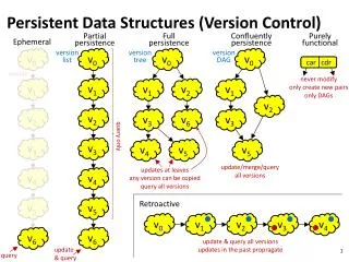
BEE3 Update: Advancements in Computer Architecture Research at Microsoft
Learn about the BEE3 project, the differences from BEE2, participants involved, engineering plan, and upcoming schedule discussed at the January 2007 RAMP Retreat. Microsoft's interest in the project, system specifications, bandwidth details, clocking, JTAG, and remaining issues addressed during the retreat.

BEE3 Update: Advancements in Computer Architecture Research at Microsoft
E N D
Presentation Transcript
BEE3 Update Chuck Thacker Technical Fellow Microsoft Research 11 January, 2007 January 2007 RAMP Retreat
Outline • What is BEE3? • BEE2-BEE3 Differences • Project participants • Engineering plan, schedule January 2007 RAMP Retreat
What is BEE3? • Follow-on to BEE2 (BWRC, 2004) • Board with several highly-connected FPGAs • Vehicle for computer architecture research • Microsoft’s primary interest • Potential platform for high performance DSP applications • Astronomers, and perhaps others. • Allows large scale architectural experiments • Although perhaps not as large as originally hoped • And certainly not at the speed of a real implementation • Can scale smoothly from a single board to 64 boards (256 FPGAs) January 2007 RAMP Retreat
BEE2 January 2007 RAMP Retreat
BEE2 – BEE3 Differences • 4 Xilinx Virtex 5 vs 5 Virtex 2 Pro FPGAs • We use XC5VLX110T-ff1136 • V2Pro is now obsolete (130nm) • V5 is a major improvement (65nm) • 6-input LUT (64 bit DP RAM) • Better Block RAMs • Improved interconnect • Better signal integrity • 8 Infiniband/CX4 channels vs 18 • 4 x8 PCI Express Low Profile slots January 2007 RAMP Retreat
BEE3 – BEE2 Differences (2) • 2 Banks DDR2 x 2 vs 4 Banks DDR2 x 1 • Same capacity (64 GB likely) • Lower bandwidth • Mandated by fewer signal pins on V5 • 4 10/100/1000 Ethernet channels • No SATA • BEE2 SATA didn’t work anyway • iSCSI instead (?) • No PowerPCs • This version has not yet been released by Xilinx January 2007 RAMP Retreat
BEE2 – BEE3 Differences (3) • Divided the system into two boards, Main and Control • Main board has FPGAs, all high speed logic • Control board handles downloading, monitoring • Simplifies main board engineering – can design control board in parallel • Smaller main board • 168 vs 374 in2 • Fewer layers for lower cost • Much more “PC-like” • Can use PC power supplies, peripherals • Several layouts are being considered • All fit in 2U enclosure • Much more attention is being given to thermal design • Must pass UL, FCC January 2007 RAMP Retreat
BEE3 Main Board January 2007 RAMP Retreat
Bandwidths (per-FPGA) • Memory • 400 MT/s * 8B/T * 2 channels: 6.4GB/s • Ring • 400 MT/s * 12 B/T: 4.8 GB/s • QSH • 400 MT/s * 10 B/T: 4 GB/s • Ethernet • 125 MB/s • CX4 • 1.25 GB/s * 2 directions * 2 channels: 5GB/s • PCI Express • Same as CX4 January 2007 RAMP Retreat
BEE3 Clocking, JTAG January 2007 RAMP Retreat
BEE3 Control Board January 2007 RAMP Retreat
BEE3 System (v1) January 2007 RAMP Retreat
BEE3 System (v2) January 2007 RAMP Retreat
BEE3 Main Board (v3) January 2007 RAMP Retreat
Remaining Issues • Precise EATX compatibility, or not? • Affects layout complexity, thermal design • Power supply sizing • We don’t want to leave the overclockers in the lurch • Standard power supplies (?) • “2U” supplies aren’t as efficient, have fewer vendors • Prefer Intel/Google “12V only” supplies (minimum loading issue), if available in time and at reasonable cost • PCI Express is nonstandard • Xilinx hard macro is “device only”, not host • Need an intrepid graduate student • Can still use it for additional Infiniband/CX4 channels January 2007 RAMP Retreat
Project Participants and Roles • Microsoft Research (Silicon Valley) • Funds and manages system engineering • Celestica (Ottawa and elsewhere) • Does main board engineering, produces final systems • Microsoft has a very deep relationship with Celestica • Function Engineering (Palo Alto) • Does thermal and mechanical engineering • Xilinx (San Jose) • Provides FPGAs for academic machines • Provides FPGA application expertise • Ramp Group (BWRC) • Control board, basic software • Ramp Community • Uses the systems for research January 2007 RAMP Retreat
Why is Microsoft interested? • We believe the overall RAMP effort will have significant impact, and want to support it in the most effective way we can. • Simply paying for grad students seems suboptimal • We observe that universities aren’t very good at this sort of system engineering and production • Grad students are great for many things, but doing things like board layout aren’t among them. • Requires deep understanding of tools and production processes. Pros have this. • We can open doors that academia can’t • We have experience in managing this sort of program • We want the systems ourselves • As infrastructure for our new effort in computer architecture (yes, this is a recruiting pitch). • We also want systems to be available to other industrial users • This might be more difficult if the systems came from academia. • But we don’t want to be in the hardware business. January 2007 RAMP Retreat
Plan, schedule • Generate design spec: 6 weeks • Scope layout problems and layer count • Layout and signal integrity: 12 weeks • Parts procurement proceeds in parallel • Will probably do 4-5 prototypes. • Board fab, test and assembly: 3 weeks • Design verification testing:5 weeks • This happens at Microsoft or BWRC • Production can start in Summer ‘07 January 2007 RAMP Retreat
Discussion? January 2007 RAMP Retreat