SOIPD Status e prospective for 2012
60 likes | 202 Vues
SOIPD Status e prospective for 2012. The SOImager2 is a monolithic pixel sensor produced by OKI in the 0.20 µm Fully Depleted-Silicon On Insulator (FD-SOI) process ; 5 5 mm 2 , 256 256 analog 3T pixels, 13.75 µm pitch , 1.8 V operational voltage; 8 different layouts;

SOIPD Status e prospective for 2012
E N D
Presentation Transcript
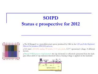
SOIPDStatus e prospective for 2012 • The SOImager2 is a monolithic pixel sensor produced by OKI in the 0.20 µm Fully Depleted-Silicon On Insulator (FD-SOI) process; • 55 mm2, 256256 analog 3T pixels, 13.75 µm pitch, 1.8 V operational voltage; 8 different layouts; • Buried P-Well process implemented: the top electronics is effectively protected from the back-gate effect (shift of top transistor threshold when a biasing voltage is applied on the backside)
Test beam with 200 GeV - at CERN SPS • Three detectors arranged in one cemented “doublet” (9 mm spaced) and one rotating plane (33 mm spaced). Singleplane can be rotated up to 20° for slanted tracks and cluster studies. • The doublet is optically aligned with a better than 50 µm precision → easy and precise coincidence cuts in cluster recognition. Plane 2 Plane 1 Cooling Plane 0 Rotating stage Beam Tracks are reconstructed in two layers (doublet) and extrapolated in the third layer (singlet). Excellent Spatial resolution and detection efficiency! Single point resolution: (1.12±0.04) μm, for Vd ≥ 50 V Detection efficiency: >99% for Vd ≥ 50 V
Back-side soft X-ray irradiation • A set of sensor chips have been back-thinned to 70 μm using a grinding technique and post-processed (P implantation followed by annealing)to create a thin entrance window (400-600nm) on the back-plane and anneal the crystal damage from the thinning; • This process ensures good sensitivity to X-rays down to ∼1.5 keVand to electrons down to ∼9 keV. • The quantum efficiency for X-rays is studied on data collected at the beam-line 5.3.1 of the Advanced Light Source (ALS) at LBNL. The thin, post-processed SOI sensor has been exposed from the backside to fluorescence radiation excited in various metal foils, in the energy range 2< E <9 keV and for 30V < Vd < 70V (Full depletion!) X-ray quantum efficiencyas a function of energy for three different values of Vd. Cluster pulse heightas a function of the energy of fluorescence X-rays obtained at Vd = 70 V. Cu spectrum 8.04keV Fe spectrum 6.4keV • precision beam monitoring in linacs and storage rings with X-rays and soft electrons. • electron microscopy • X-ray astronomy • … Possible applications for pixellated sensors with large quantum efficiency for soft X-rays and low-energy particles, small pixels, fast readout and moderate energy resolution are:
Single Event Upset tests Shift register layout • Single Event Upset (SEU) micrometric sensitivity studies on the digital circuitry of the chip were performed at the Ion Electron Emission Microscope (IEEM) facility, located at the 15MV Tandem XTU-Accelerator of the INFN Legnaro National Laboratory • A known logical pattern is written in and read back from the row selection shift register through dedicated pads during irradiation. Differences between the loaded and read-back pattern highlight a SEU occurred in the cells latch latch 256 shift register (SR) cells, 13.75 µm pitch 22.4m 250 MeV 79Br • Four pairs of hot spots: each pair corresponds to a single SR cell and the two spots highlight the two Flip-Flop D structure of the cell. • The different number of upset in the two columns of spots accounts for the dependence of the sensitivity from the logic state of the Flip-Flop
Activity for 2012 • Test of the new, larger chip built on Float Zone (FZ) SOI wafers with resistivity of several 1000 ·cm, recently made available from OKI; this chip can achieve full depletion on a thickness up to 500 m. • Test beam at CERN SPS with - on a chip back-thinned and back-processed • Test of a back-thinned and back-processed chip with low energy electrons (10-20 keV)
Personnel and budget request for 2012 Richieste economiche: Missioni interne: 1k€ Missioni estere: 4k€ Consumo: 2k€ Personnel: D. Bisello 30% S. Mattiazzo 70% R. Rando 30% L. Silvestrin 30% M. Bagatin (DEI) 30% Technical assistance: D. Pantano 50%
