HFT PIXEL detector LVDS Data Path Testing
HFT PIXEL detector LVDS Data Path Testing. Outline. Review of RDO design. LVDS Data Path test design Status. For more information, please see: http://rnc.lbl.gov/hft/hardware/docs/LVDS/index.html. Phase-1 Sensor characteristics. 640 x 640 array – 30 micron pixels

HFT PIXEL detector LVDS Data Path Testing
E N D
Presentation Transcript
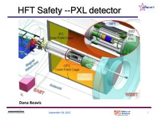
HFT PIXEL detector LVDS Data Path Testing Leo Greiner PIXEL Hardware meeting 2007-12-13
Outline • Review of RDO design. • LVDS Data Path test design • Status For more information, please see: http://rnc.lbl.gov/hft/hardware/docs/LVDS/index.html Leo Greiner PIXEL Hardware meeting 2007-12-13
Phase-1 Sensor characteristics • 640 x 640 array – 30 micron pixels • On-chip CDS and discriminators • 4 LVDS outputs / sensor • Rolling shutter readout – binary digital data per pixel • 640 microsecond integration time • 160 MHz LVDS RDO clock speed (this is configurable) The Ultimate sensor will have on chip zero-suppression and 1 output / sensor. The readout clock can be slower than the 160 MHz required for the Phase-1. Leo Greiner PIXEL Hardware meeting 2007-12-13
RDO System Design – System Blocks • This is a highly parallel system – a schematic representation is shown below. Leo Greiner PIXEL Hardware meeting 2007-12-13
Sensors, Ladders, Carriers (interaction point) LU Protected Regulators, Mass cable termination RDO Boards DAQ PCs RDO System Design – Physical Layout 1 m – Low mass twisted pair 30 m Power Supplies Platform 6 m - twisted pair 100 m - Fiber optic cables Magnet Pole Face (Low Rad Area) DAQ Room Leo Greiner PIXEL Hardware meeting 2007-12-13
Detailed RDO System Structure – Sensors and Cables Early prototype cable with 40 differential pair output, clock and control routed under sensor area. Fine twisted pair cables 125 micron diameter wire Soldered directly to cable Low stiffness / mass • 4 LVDS outputs / sensor • Cable • 4 layer - 150 micron thickness • Aluminum Conductor • Radiation Length ~ 0.1 % • 40 LVDS pair signal traces • Clock, JTAG, sync, marker Leo Greiner PIXEL Hardware meeting 2007-12-13
Detailed RDO System Structure – LU Protection and Mass Termination 1 Main Board per carrier 10 carriers in the PIXEL detector Leo Greiner PIXEL Hardware meeting 2007-12-13
Detailed RDO System Structure – RDO Board(s) Two board System – Virtex-5 Development board mated to a new HFT motherboard Xilinx Virtex-5 Development Board New motherboard • Digital I/O LVDS Drivers • 4 X >80 MHz ADCs • PMC connectors for SIU • Cypress USB chipset • SODIMM Memory slot • Serial interface • Trigger / Control input Note – This board is designed for development and testing. Not all features will be loaded for production. • FF1760 Package • 800 – 1200 I/O pins • 4.6 – 10.4 Mb block RAM • 550 MHz internal clock Leo Greiner PIXEL Hardware meeting 2007-12-13
Data Path LVDS Test Block Diagram Leo Greiner PIXEL Hardware meeting 2007-12-13
Testing Plan • Bit Error Rate and Eye Pattern Plots for combinations of: • Different cable types from the Mass-termination board to the V5 interface board. • Different cable lengths from the Mass-termination board to the V5 interface board. • Range of clock RDO frequencies including pseudo random data and clock data. • Hardware configuration either straight path through Mass-termination board or through buffers. Leo Greiner PIXEL Hardware meeting 2007-12-13
Status • Virtex-5 Development Board – in hand and ready for testing. • Ladder test board – Layout completed. Soliciting quotations for PCB fabrication. • Mass-termination board – in Layout. • V5 interface board – Schematic complete. Ready for layout. We anticipate being ready to begin testing in mid January. Leo Greiner PIXEL Hardware meeting 2007-12-13
fin Leo Greiner PIXEL Hardware meeting 2007-12-13
Detailed System Structure – RDO Functional Data Path – Phase 1 Leo Greiner PIXEL Hardware meeting 2007-12-13
Data Rates - Parameters Radius R = 2.5 R = 8.0 • Rates as per Jim Thomas, L = 3 x 1027 for Phase-1, L = 8 x 1027 for Ultimate. • 2.5 hits / cluster. • 1 kHz average event rate. • 10 inner ladders, 30 outer ladders. • Factor of 1.6 for event format overhead (can be lowered). • No run length encoding. 200 us Integration Time Hits / Sensor at L = 8 x 1027. 640 us Leo Greiner PIXEL Hardware meeting 2007-12-13
Data Rates • Ultimate => 49.7 MB / s raw addresses. => 79.5 MB / s data rate. • Phase–1 => 59.6 MB / s raw addresses => 95.4 MB / s data rate. The dead-time is primarily limited by the number of externally allocated readout buffers! Leo Greiner PIXEL Hardware meeting 2007-12-13