Photoelectric effect explained
180 likes | 223 Vues
Photoelectric effect explained. But now, a behavior of light was observed that fit Planck ’ s energy packet idea. So electromagnetic radiation appears to behave as if it is both a wave and a particle.

Photoelectric effect explained
E N D
Presentation Transcript
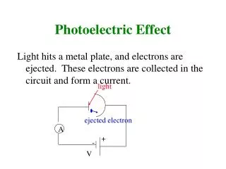
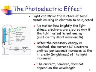
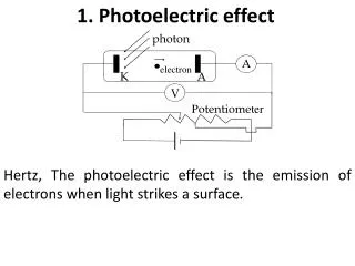
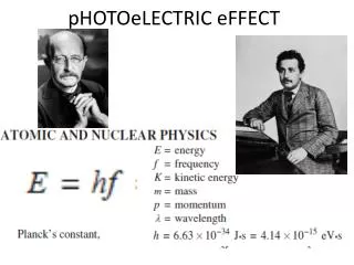
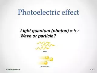
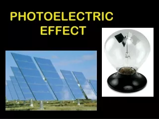
Photoelectric effect explained • But now, a behavior of light was observed that fit Planck’s energy packet idea. • So electromagnetic radiation appears to behave as if it is both a wave and a particle. • In fact, you can think of light as discrete wave packets-packets of waves which, depending upon the measurement you make, sometimes exhibit particle behavior and sometimes exhibit wave behavior. • Einstein won the Nobel prize for his explanation of the photoelectric effect.
Semi conductors • Devices which have conductive properties in between a conductor and an insulator. • Normally, the outer (valence) electrons are tightly bound to the nucleus and cannot move. • If one or all of them could be freed up, then the material can conduct electricity • Silicon is an example of a semi-conductor.
Silicon • Element 14 in the periodic table • Very common element (sand, glass composed of it) • 8th most common element in the universe • Its 4 outer valence electrons are normal tightly bound in the crystal structure. • However, when exposed to light, the outer electrons can break free via the photoelectric effect and conduct electricity. • For silicon, the maximum wavelength to produce the photoelectric effect is 1.12 microns. 77% of sunlight is at wavelengths lower than this.
But its not quite this simple • You also need to produce a voltage within the silicon to drive the current. • So the silicon must be combined with another material. This process is called doping. • 2 types of doping: P and N • If you replace one of the silicon atoms in the crystal lattice with a material that has 5 valence electrons, only 4 are need to bond to the lattice structure, so one remains free. The doped semi conductor has an excess of electrons and is called an N type semiconductor. • Doping elements can be arsenic, antimony or phosphorus.
P-types • If you dope with an element with only 3 valence electrons, there is a vacancy, or hole left where the 4th electron should be. • If the hole becomes occupied by an electron from a neighbor atom, the hole moves through the semiconductor. This acts like a current with positive charge flowing through the semi conductor, so it appears to have a net positive charge • Called a P-type semiconductor. • Doping elements could be boron, aluminum, or indium
Creating the solar cell • To create the solar cell, bring a p-type silicon into contact with an n-type silicon. • The interface is called a p-n junction. • Electrons will diffuse from the n material to the p material to fill the holes in the p material. This leaves a hole in the n material. • So the n-material ends up with an excess positive charge and the p material ends up with an excess negative charge. • This creates an electric field across the junction.
Current in the solar cell • Any free electrons in the junction will move towards the n –type material and any holes will move toward the p -type material . • Now sunlight will cause the photoelectric effect to occur in the junction. Thus free electrons and holes are created in the junction and will move as described above. • Current flows!
Solar Cells • Typically 2 inches in diameter and 1/16 of an inch thick • Produces 0.5 volts, so they are grouped together to produce higher voltages. These groups can then be connected to produce even more output. • In 1883 the first solar cell was built by Charles Fritts. He coated the semiconductor selenium with an extremely thin layer of gold to form the junctions. The device was only around 1% efficient.
Generations of Solar cells • First generation • large-area, high quality and single junction devices. • involve high energy and labor inputs which prevent any significant progress in reducing production costs. • They are approaching the theoretical limiting efficiency of 33% • achieve cost parity with fossil fuel energy generation after a payback period of 5-7 years. • Cost is not likely to get lower than $1/W.
Generations of Solar cells • Second generation-Thin Film Cells • made by depositing one or more thin layers (thin film) of photovoltaic material on a substrate. • thickness range of such a layer varies from a few nanometers to tens of micrometers. • Involve different methods of deposition: • Chemical Vapor deposition the wafer (substrate) is exposed to one or more volatile precursors, which react and/or decompose on the substrate surface to produce the desired deposit. Frequently, volatile by-products are also produced, which are removed by gas flow through the reaction chamber.
Thin Film deposition techniques • Electroplating • electrical current is used to reduce cations (positively charged ions) of a desired material from a solution and coat a conductive object with a thin layer of the material. • Ultrasonic nozzle • spray nozzle that utilizes a high (20 kHz to 50 kHz) frequency vibration to produce a narrow drop size distribution and low velocity spray over the wafer • These cells are low cost, but also low efficiency
The Third Generation • Also called advanced thin-film photovoltaic cell • range of novel alternatives to "first generation” and "second generation” cells. • more advanced version of the thin-film cell.
Third generation alternatives • non-semiconductor technologies (including polymer cells and biomimetics) • quantum dot technologies • also known as nanocrystals, are a special class semiconductors. which are crystals composed of specific periodic table groups. Size is small, ranging from 2-10 nanometers (10-50 atoms) in diameter. • tandem/multi-junction cells • multijunction device is a stack of individual single-junction cells • hot-carrier cells • Reduce energy losses from the absorption of photons in the lattice • upconversion and downconversion technologies • Put a substance in front of the cell that converts low energy photons to higher energy ones or higher energy photons to lower energy ones that the solar cells can convert to electricity. • solar thermal technologies, such as thermophotonics(TPX) • A TPX system consists of a light-emitting diode (LED) (though other types of emitters are conceivable), a photovoltaic (PV) cell, an optical coupling between the two, and an electronic control circuit. The LED is heated to a temperature higher than the PV temperature by an external heat source. If power is applied to the LED, , an increased number of electron-hole pairs (EHPs) are created.These EHPs can then recombine radiatively so that the LED emits light at a rate higher than the thermal radiation rate ("superthermal" emission). This light is then delivered to the cooler PV cell over the optical coupling and converted to electricity.
Efficiency and cost factors • Average cost per peak watt is $1.00-$3.00. Coal fired plant is $1.00/watt. • Efficiency is not great. • Recall, 77% of the incident sunlight can be used by the cell. • 43% goes into heating the crystal. • Remaining efficiency is temperature dependent • Average efficiency of a silicon solar cell is 14-17% • The second and third generation technologies discussed are designed to increase these efficiency numbers and reduce manufacturing costs
Novel approaches • UA astronomer Roger Angel • Uses cheap mirrors to focus sunlight on 3rd generation solar cells (triple junction cells) which handle concentrated light • $1.00 per watt achievable-competitive with coal plants • Potential: 1 solar farm 100 miles on a side could provide electricity to the whole nation • Does not have to be all in one place
Solar Cooling • Consider a refrigeration system with no moving parts. • Heat the coolant (say ammonia gas dissolved in water) and force it via a generator into an evaporator chamber where it expands into a gas and cools. Move it to a condenser and cool it back to a liquid and repeat the process. • These systems actually have existed for a number of years, refrigerators in the 1950s were sold with this technology (gas powered and there was/is a danger of CO emissions). • Energy to heat the coolant and drive it through the system comes from burning fuel or a solar cell to provide electricity to do the heating. • Need what is called a concentrating collector (lens or other system to concentrate more light on the solar cell). • Ideally, you could do this with a flat plate collector system, though you do not obtain as much cooling. • Devices are not widely used, due to the intermittency of sunlight
