Download
1 / 17
170 likes | 290 Vues
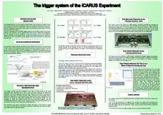
This document presents the design and implementation of the trigger system used in the MEG experiment, led by D. Nicolò F. Morsani, S. Galeotti, and Marco Grassi from INFN-Pisa. It details the expected trigger rate, accidental background, and rejection criteria based on variables such as photon energy, direction, positron interactions, and time correlation. The system utilizes digital technology, including Flash analog-to-digital converters (FADC) and FPGAs, with a tree-structured board layout facilitating efficient data processing and remote debugging capabilities. Final tests confirm a satisfactory performance meeting all experimental requirements.

E N D
The Trigger System of the MEG Experiment On behalf of D. Nicolò F. Morsani S. Galeotti Marco Grassi INFN - Pisa
Expected Trigger Rate Accidental background and Rejection obtained by applying cuts on the following variables • photon energy • photon direction • hit on the positron counter • time correlation • positron-photon direction match The rate depends on RRe+ R2
The trigger implementation Digital approach • Flash analog-to-digital converters (FADC) • Field programmable gate array (FPGA) Final system • Only 2 different board types • Arranged in a tree structure on 3 layers • Connected with fast LVDS buses • Remote configuration/debugging capability Prototype board Check of: • the FADC-FPGA compatibility • chosen algorithms • synchronous operation • data transmission
LVDS Rec Analog receivers 16 x 10 PMT FADC FPGA 16 Clock Sync Trigger Start Out 4 4 16 16 48 Control CPLD 4 3 48 4 48 Sync Trigger Start Sync 2 boards Spare in/out Type0 Type0 VME Trigger Start LVDS Trans Prototype board : Type 0 • VME 6U • A-to-D Conversion • Trigger • I/O • 16 PMT signals • 2 LVDS transmitters • 4 in/2 out control signals • Complete system test Board Type0
The board control signals. LVDS transm. Differential drivers PMT inputs FPGA FADC LVDS receiv. configuration EPROMS package error solved with a patch board
Prototype system Two identical Type0 boards Board 0 Board 1 Ancillary board Clock, sync, trigger and start distribution LVDS connection
Circ. buff Circ. buff Circ. buff Circ. buff Diff. driver Diff. driver Proc. Algor. Proc. Algor. Fadc Fadc LVDS Tx LVDS Tx Proc. Algor. Proc. Algor. LVDS Rx LVDS Rx Circ. buff Circ. buff Circ. buff Circ. buff Board 1 Prototype system configuration input output 16 PMT Board 0 16 PMT input output LVDS in final
Prototype system tests • Debugging of the first board Type0 in Pisa • A minor error fixed • System assembled at PSI in Nov. ‘03 • 100MHz synchronous operation • Negligible transmission error rate • Satisfactory operation of the analog interface • Connection with the Large Prototype • PMT from #0 to #31 • Collected data • Alpha • Led • 0
Alpha Amplitude [mV] Input cyclic-buffer board 1 Time [10 ns]
LED Amplitude [mV] Time [10 ns]
0 Amplitude [mV] Time [10 ns]
Internal trigger Pulse time Output cyclic-buffer board 0 Input cyclic-buffer board 0 Amplitude [mV] Amplitude sum Index of Max Max. Amplitude (2) Time [10 ns]
LVDS transmission Pulse time Amplitude [mV] Output cyclic-buffer board 1 LVDS input cyclic-buffer board 0 Amplitude sum Index of Max Max. Amplitude (2) Time [10 ns] 7 clock cycles delay
Example of data comparison • 0 data • Charge spectrum • Only 32 PMT
Further works • Hardware • JTAG programming/debugging through VME by modifying the Type0 • Block transfer in A32D16 format (VME library to be modified) • Final characterization on linearity, crosstalk … • Analysis • Alpha, Led and 0data to extensively check the algorithms Conclusions The prototype system met all requirements It is available to trigger the LP in future beam tests
Final system • Trigger location: platform • Spy buffers to check the data flow are implemented • JTAG programming/debugging through VME: test planned with Type0 • Final boards • VirtexII or Spartan3 ? • MainFPGAXCV812E-8-FG900 is old, first production in 2000 • Connectors • Analog input by3M coaxialconnectors • LVDS connection by3M cables • Differential driver on the trigger board Type1 • Other components are fixed: FADC, LVDS Tx and Rx, Clock distributor • Ancillary boards: distribution of control signals • Design of final prototypes (Type1 and Type2) june 2004 • If tests are okstart of the mass production • Estimated production and test 1 year
Jan 2002 Trigger 2002 2003 2004 2005 Prototype Board Final Prototype Full System now Design Manufactoring Assembly Test Milestone