
SlideServe
Menu
Préférences
© SlideServe · v2026

Antireflective SiC Surface Fabrication via Plasma Etching and Self-Assembled Nanopatterns

hong avatar
1 diapositives · 166 Views · Oct 15, 2014

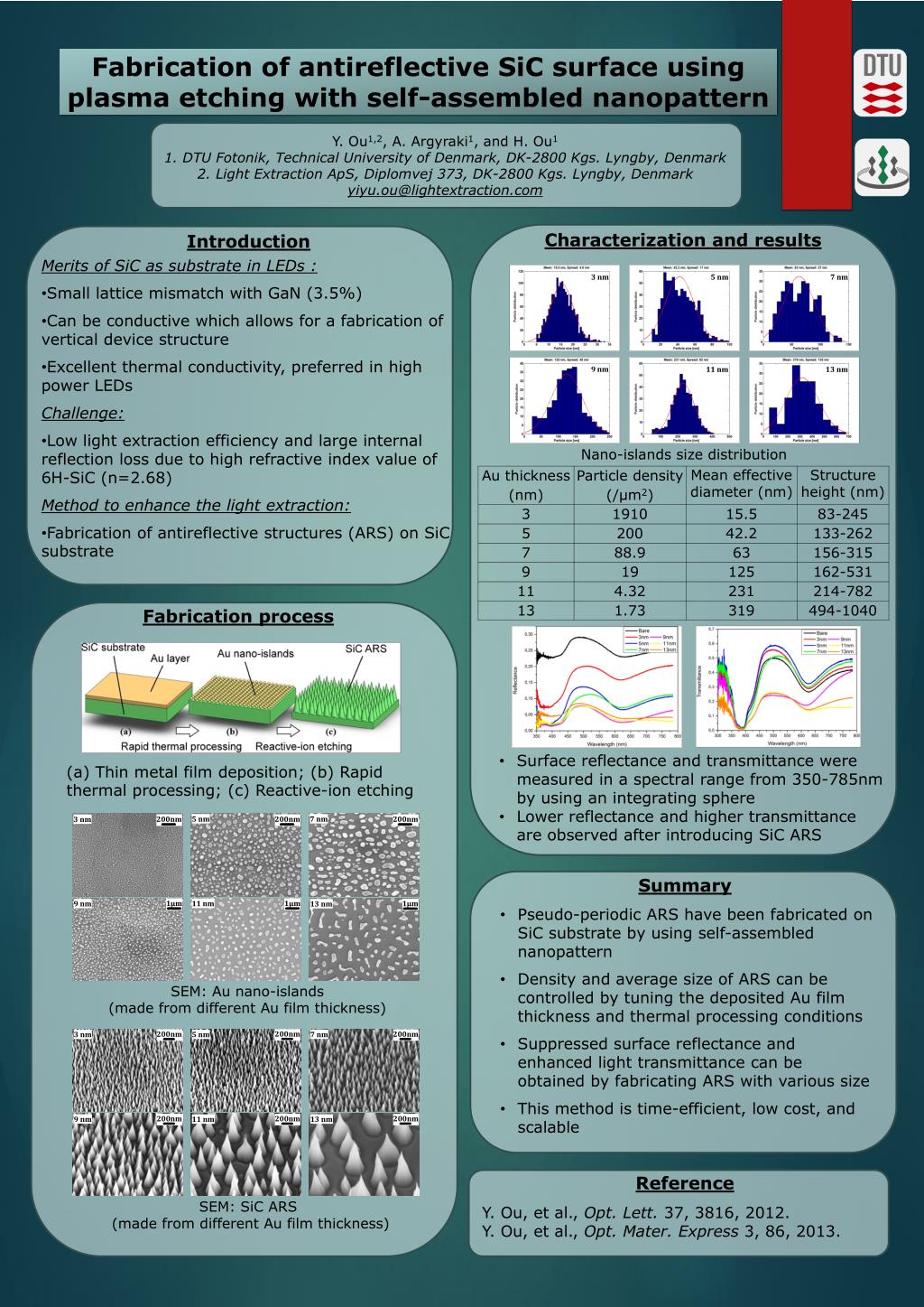
This study presents an innovative method for fabricating antireflective structures on SiC substrates using plasma etching and self-assembled nanostructures. SiC's unique properties offer advantages in LED technology; however, its high refractive index results in low light extraction efficiency. By creating pseudo-periodic antireflective structures (ARS) through controlled deposition of gold films and thermal processing, we achieved significant reductions in surface reflectance and enhanced light transmission. This approach is low-cost, time-efficient, and scalable, making it suitable for advanced LED applications.
Antireflective SiC Surface Fabrication via Plasma Etching and Self-Assembled Nanopatterns - slide 1
01 / 1Antireflective SiC Surface Fabrication via Plasma Etching and Self-Assembled Nanopatterns
1 / 17

Télécharger la présentation

Antireflective SiC Surface Fabrication via Plasma Etching and Self-Assembled Nanopatterns
Une image / un lien ci-dessous est fourni (tel quel) pour télécharger la présentation

Politique de téléchargement : le contenu du site vous est fourni TEL QUEL pour votre information et votre usage personnel ; il ne peut être vendu, concédé sous licence ni partagé sur d’autres sites sans l’accord de son auteur.Le contenu vous est fourni TEL QUEL, pour votre information et votre usage personnel uniquement. Téléchargez la présentation en cliquant sur ce lien. Lors du téléchargement, si vous ne parvenez pas à télécharger une présentation, l’éditeur a peut-être supprimé le fichier de son serveur.Pendant le téléchargement, si vous ne parvenez pas à obtenir une présentation, le fichier a peut-être été supprimé par l’éditeur.

F I N

Plus de contenu associé

Transcription de la présentation
  1. Fabrication of antireflective SiC surface using plasma etching with self-assembled nanopattern Y. Ou1,2, A. Argyraki1, and H. Ou1 1. DTU Fotonik, Technical University of Denmark, DK-2800 Kgs. Lyngby, Denmark 2. Light Extraction ApS, Diplomvej 373, DK-2800 Kgs. Lyngby, Denmark yiyu.ou@lightextraction.com Characterization and results Introduction • Merits of SiC as substrate in LEDs : • Small lattice mismatch with GaN (3.5%) • Can be conductive which allows for a fabrication of vertical device structure • Excellent thermal conductivity, preferred in high power LEDs • Challenge: • Low light extraction efficiency and large internal reflection loss due to high refractive index value of 6H-SiC (n=2.68) • Method to enhance the light extraction: • Fabrication of antireflective structures (ARS) on SiC substrate 5 nm 7 nm 3 nm 9 nm 11 nm 13 nm Nano-islands size distribution Fabrication process • Surface reflectance and transmittance were measured in a spectral range from 350-785nm by using an integrating sphere • Lower reflectance and higher transmittance are observed after introducing SiC ARS 200nm (a) Thin metal film deposition; (b) Rapid thermal processing; (c) Reactive-ion etching 5 nm 7 nm 200nm 200nm 3 nm Summary • Pseudo-periodic ARS have been fabricated on SiC substrate by using self-assembled nanopattern • Density and average size of ARS can be controlled by tuning the deposited Au film thickness and thermal processing conditions • Suppressed surface reflectance and enhanced light transmittance can be obtained by fabricating ARS with various size • This method is time-efficient, low cost, and scalable 9 nm 11 nm 13 nm 1µm 1µm 1µm SEM: Au nano-islands (made from different Au film thickness) 5 nm 7 nm 3 nm 200nm 200nm 200nm 200nm 200nm 200nm 9 nm 11 nm 13 nm Reference Y. Ou, et al., Opt. Lett. 37, 3816, 2012. Y. Ou, et al., Opt. Mater. Express 3, 86, 2013. SEM: SiC ARS (made from different Au film thickness)