Download
1 / 26
270 likes | 447 Vues
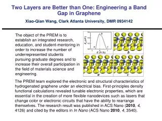
Scaling First Principles Materials and Nanoscience Codes to Thousands of Processors (and Thousands of Atoms). (Plane-wave, DFT codes). Andrew Canning and Lin-Wang Wang Computational Research Division LBNL. Electron Wavefunction. Nanostructure. Both are in nanometers. size.

E N D
Scaling First Principles Materials and Nanoscience Codes to Thousands of Processors (and Thousands of Atoms) (Plane-wave, DFT codes) Andrew Canning and Lin-Wang Wang Computational Research Division LBNL
Electron Wavefunction Nanostructure Both are in nanometers size Nanostructures as a new material Definition: Nanostructure is an assembly of nanometer scale “building blocks”. Why nanometer scale: This is the scale when the properties of these “building blocks” become different from bulk.
Example: Quantum Dots (QD) CdSe • Band gap increase CdSe quantum dot (size) • Single electron effects • on transport (Coulomb • blockade). • Mechanical properties, • surface effects and no • dislocations
atoms nanostructures bulk molecules Computational challenges (larger nanostructures) Infinite (1-10 atoms in a unit cell) 1-100 atoms 1000-10^6 atoms size • Ab initio method • PARATEC Challenge for computational nanoscience. Ab initio Method PARATEC method • Effective mass • method Ab initio elements and reliability New methodology and algorithm (ESCAN) Even larger Supercomputer
Plane-wave Pseudopotential Method in DFT Solve Kohn-Sham Equations self-consistentlyfor electron wavefunctions 1. Plane-wave expansion for 2. Replace “frozen” core by a pseudopotential Different parts of the Hamiltonian calculated in different spaces (fourier and real) 3d FFT used
Parallel Algorithm Details • Divide sphere of plane-waves in columns between processors (planes of grid in real space) • Parallel 3d FFT used to move between real space and fourier space • FFT requires global communications data packet size ~ 1/(# processors)^2
Parallel 3D FFT (a) (b) • 3D FFT done via 3 sets of 1D FFTs and 2 transposes • Most communication in global transpose (b) to (c) little communication (d) to (e) • Flops/Comms ~ logN • Many FFTs done at the same time to avoid latency issues • Only non-zero elements communicated/calculated • Much faster than vendor supplied 3D-FFT (c) (d) (e) (f)
How to scale up the parallel 3d FFTs • Minimize the global communications part • Latency problem: Use all-band method in conjunction with many FFTs at the same time to make data packets larger (new all band CG method for metals ) • FFT part scales as N logN while other parts scale as N (larger systems scale better) 2 3
Materials/Nanoscience codes Parallel Fourier techniques (many-band approach) used in the following codes: • PARATEC PARAllel Total Energy Code (plane-wave pseudopotential code) • PEtot (plane-wave ultrasoft pseudopotential code) • ESCAN (Energy SCAN) Uses folded spectrum method for non-selfconsistent nanoscale calculations with plane-waves for larger systems.
PARATEC (PARAllel Total Energy Code) • PARATEC performs first-principles quantum mechanical total energy calculation using pseudopotentials & plane wave basis set • Designed to run on large parallel machines IBM SP etc. but also runs on PCs • PARATEC uses all-band CG approach to obtain wavefunctions of electrons • Generally obtains high percentage of peak on different platforms • Developed with Louie and Cohen’s groups (UCB, LBNL), Raczkowski (Multiple 3d FFTs Peter Haynes and Michel Cote)
PARATEC: Performance 432Si-atomsystem with5CG steps 432 Atom Si Bulk System 5 CG step • First time code achieved over 1 TflopAggregate 2.6 TFlops for 686 Si atom • Previous best was .7 TFlop on Power3 using 1500 procs Work carried out with L. Oliker (CRD) J.T. Carter (NERSC)
PARATEC: Performance on ES SX6 Scaling Issues 686 atom Si • % time in communications increasing (3D FFT) • Fewer number of multiple 1D FFTs for each proc. (vector length drops) • Matrices for BLAS3 becoming smaller (vector length drops)
PARATEC: Scaling ES vs. Power3 • ES can run the same system about 10 times faster than the IBM SP (on any number of processors) • Main advantage of ES for these types of codes is the fast communication network • Fast processors require less fine-grain parallelism in code to get same performance as RISC machines • QD is 309 atom CdSe Quantum Dot
Applications: Free standing quantum dots (CdSe) CdSe quantum dot TEM image • Chemically synthesised (Alivisatos, UCB, LBNL) • Interior atoms are in bulk crystal structure • Surface atoms are passivated • Diameter ~ 20-100 A • A few thousand atoms, beyond ab initio method
CdSe quantum dots as biological tags • Optically more stable than dye molecules • Can have multiple colors
atoms nanostructures bulk molecules Computational challenges (larger nanostructures) Infinite (1-10 atoms in a unit cell) 1-100 atoms 1000-10^6 atoms size • Ab initio method • PARATEC Challenge for computational nanoscience. Ab initio Method PARATEC method • Effective mass • method Ab initio elements and reliability New methodology and algorithm (ESCAN) Even larger Supercomputer
Charge patching method for larger systems (L-W. Wang) Non-selfconsistent LDA quality potential for nanotube Selfconsistent LDA calculation of a single graphite sheet Get information from small system ab initio calc., then generate the charge densities for large systems
Plane-wave Pseudopotential Method in DFT Solve Kohn-Sham Equations non-selfconsistentlyfor electron wavefunctions in desired energy range using patched charge density (can study larger nanosystems 10,000 atoms) 1. Plane-wave expansion for 2. Replace “frozen” core by a pseudopotential Different parts of the Hamiltonian calculated in different spaces (fourier and real) 3d FFT used
Motif based charge patching method Error: 1%, ~20 meV eigen energy error.
N + Folded Spectrum Method (ESCAN)
Charge patching: free standing quantum dots In675P652 LDA quality calculations (eigen energy error ~ 20 meV) 64 processors (IBM SP3) for ~ 1 hour Total charge density motifs CBM VBM
Polarization of CdSe quantum rods CdSe quantum rods The electron wavefunctions of a quantum rods
GaN (111) and (112) quantum wires (WZ) (111) GaN wire (112) GaN wire CB1 CB2
Conclusion First principles calculation New algorithm methodology Large scale supercomputer + + Million atom nanostructures
Acknowledgements • This research was in part funded by the DOE as part of the Modeling and Simulation in Nanoscience Initiative (MICS and BES) • This research used resources of NERSC at LBNL ad CCS at ORNL supported under contract No DE-AC03-76SF00098 and DE-AC05-00OR22725. • The authors were in part supported by the Office of Advanced Scientific Computing Research in the DOE Office of Science under contract number DE-AC03-76SF00098 • A. Canning would like to thank the staff of the Earth Simulator Center, especially Dr. T. Sato, S. Kitawaki Y. Tsuda and D. Parks, J. Snyder (NEC, USA) for their assistance during his visit.