Download
1 / 1
10 likes | 111 Vues
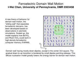
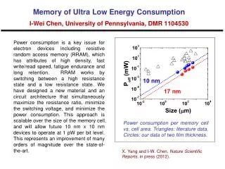
This research by I-Wei Chen at University of Pennsylvania focuses on reducing power consumption in resistive random access memory (RRAM) devices. The new material and circuit architecture aim to maximize resistance ratio, minimize switching voltage, and lower power usage. The approach is scalable, enabling future 10 nm x 10 nm devices to operate at 1 pW per bit level, a significant advancement over current technology. The study compares power consumption per memory cell with cell area, showcasing substantial improvements. Findings are detailed in Yang and Chen's 2012 publication in Nature Scientific Reports.

E N D
Memory of Ultra Low Energy ConsumptionI-Wei Chen, University of Pennsylvania, DMR 1104530 Power consumption is a key issue for electron devices including resistive random access memory (RRAM), which has attributes of high density, fast write/read speed, fatigue endurance and long retention. RRAM works by switching between a high resistance state and a low resistance state. We have designed a new material and an circuit architecture that simultaneously maximize the resistance ratio, minimize the switching voltage, and minimize the power consumption. This approach is scalable over the size of the memory cell, and will allow future 10 nm x 10 nm devices to operate at 1 pW per bit level. This represents an improvement of many orders of magnitude over the state-of-the-art. Power consumption per memory cell vs. cell area. Triangles: literature data. Circles: our data of two film thickness. X. Yang and I-W. Chen, Nature Scientific Reports, in press (2012).