Memory Hierarchy Design
Memory Hierarchy Design. Outline. Introduction Reviews of the ABCs of caches Cache Performance Reducing Cache Miss Penalty Reducing Miss Rate Reducing Cache Miss Penalty or Miss Rate Via Parallelism Reducing Hit Time Main Memory and Organizations for Improving Performance


Memory Hierarchy Design
E N D
Presentation Transcript
Outline • Introduction • Reviews of the ABCs of caches • Cache Performance • Reducing Cache Miss Penalty • Reducing Miss Rate • Reducing Cache Miss Penalty or Miss Rate Via Parallelism • Reducing Hit Time • Main Memory and Organizations for Improving Performance • Memory Technology • Virtual Memory • Protection and Examples of Virtual Memory • Assignment Questions
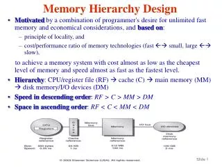
Memory Hierarchy Design • Motivated by the principle of locality - A 90/10 type of rule • Take advantage of 2 forms of locality • Spatial - nearby references are likely • Temporal - same reference is likely soon • Also motivated by cost/performance structures • Smaller hardware is faster: SRAM, DRAM, Disk, Tape • Access vs. bandwidth variations • Fast memory is more expensive • Goal – Provide a memory system with cost almost as low as the cheapest level and speed almost as fast as the fastest level
DRAM/CPU Gap • CPU performance improves at 55%/year • In 1996 it was a phenomenal 18% per month • DRAM - has improved at 7% per year
Cache • The first level of the memory hierarchy encountered once the address leaves the CPU • Persistent mismatch between CPU and main-memory speeds • Exploit the principle of locality by providing a small, fast memory between CPU and main memory -- the cache memory • Cache is now applied whenever buffering is employed to reuse commonly occurring terms (ex. file caches) • Caching – copying information into faster storage system • Main memory can be viewed as a cache for secondary storage
General Hierarchy Concepts • At each level - block concept is present (block is the caching unit) • Block size may vary depending on level • Amortize longer access by bringing in larger chunk • Works if locality principle is true • Hit - access where block is present - hit rate is the probability • Miss - access where block is absent (in lower levels) - miss rate • Mirroring and consistency • Data residing in higher level is subset of data in lower level • Changes at higher level must be reflected down - sometime • Policy of sometime is the consistency mechanism • Addressing • Whatever the organization you have to know how to get at it! • Address checking and protection
Physical Address Structure • Key is that you want different block sizes at different levels
Latency and Bandwidth • The time required for the cache miss depends on both latency and bandwidth of the memory (or lower level) • Latency determines the time to retrieve the first word of the block • Bandwidth determines the time to retrieve the rest of this block • A cache miss is handled by hardware and causes processors following in-order execution to pause or stall until the data are available
Predicting Memory Access Times • On a hit: simple access time to the cache • On a miss: access time + miss penalty • Miss penalty = access time of lower + block transfer time • Block transfer time depends on • Block size - bigger blocks mean longer transfers • Bandwidth between the two levels of memory • Bandwidth usually dominated by the slower memory and the bus protocol • Performance • Average-Memory-Access-Time = Hit-Access-Time + Miss-Rate * Miss-Penalty • Memory-stall-cycles = IC * Memory-reference-per-instruction * Miss-Rate * Miss-Penalty
Headaches of Memory Hierarchies • CPU never knows for sure if an access will hit • How deep will a miss be - i. e. miss penalty • If short then the CPU just waits • If long then probably best to work on something else – task switch • Implies that the amount can be predicted with reasonable accuracy • Task switch better be fast or productivity/efficiency will suffer • Implies some new needs • More hardware accounting • Software readable accounting information (address trace)
Four Standard Questions • Block Placement • Where can a block be placed in the upper level? • Block Identification • How is a block found if it is in the upper level? • Block Replacement • Which block should be replaced on a miss? • Write Strategy • What happens on a write? Answer the four questions for the first level of the memory hierarchy
Block Placement Options • Direct Mapped • (Block address) MOD (# of cache blocks) • Fully Associative • Can be placed anywhere • Set Associative • Set is a group of n blocks -- each block is called a way • Block first mapped into a set (Block address) MOD (# of cache sets) • Placed anywhere in the set • Most caches are direct mapped, 2- or 4-way set associative
Block Placement Options (Cont.) Continuum of levels of set associativity (m=0) (m=3) (m=2)
Block Identification Many memory blocks may map to the same cache block • Each cache block carries tags • Address Tags: which block am I? • Physical address now: address tag## set index## block offset • Note relationship of block size, cache size, and tag size • The smaller the set tag the cheaper it is to find • Status Tags: what state is the block in? • valid, dirty, etc. Physical address =r + m + n bits r (address tag) m (set index) n(block offset) 2m addressable sets in the cache 2n bytesper block
Block Identification (Cont.) Physical address = r + m + n bits r (address tag) m n 2m addressable sets in the cache 2n bytesper block • Caches have an address tag on each block frame that gives the block address. • A valid bit to say whether or not this entry contains a valid address. • The block frame address can be divided into the tag filed and the index field.
Block Replacement • Random: just pick one and chuck it • Simple hash game played on target block frame address • Some use truly random • But lack of reproducibility is a problem at debug time • LRU - least recently used • Need to keep time since each block was last accessed • Expensive if number of blocks is large due to global compare • Hence approximation is often used = Use bit tag and LFU • FIFO Only one choice for direct-mappedplacement
Data Cache Misses Per 1000 Instructions 64 byte blocks on a Alpha using 10 SPEC2000
Short Summaries from the Previous Figure • More-way associative is better for small cache • 2- or 4-way associative perform similar to 8-way associative for larger caches • Larger cache size is better • LRU is the best for small block sizes • Random works fine for large caches • FIFO outperforms random in smaller caches • Little difference between LRU and random for larger caches
Improving Cache Performance • MIPS mix is 10% stores and 37% loads • Writes are about 10%/(100%+10%+37%) = 7% of overall memory traffic, and 10%/(10%+37%)=21% of data cache traffic • Make the common case fast • Implies optimizing caches for reads • Read optimizations • Block can be read concurrent with tag comparison • On a hit the read information is passed on • On a miss the - nuke the block and start the miss access • Write optimizations • Can’t modify until after tag check - hence take longer
Write Options • Write through: write posted to cache line and through to next lower level • Incurs write stall (use an intermediate write buffer to reduce the stall) • Write back • Only write to cache not to lower level • Implies that cache and main memory are now inconsistent • Mark the line with a dirty bit • If this block is replaced and dirty then write it back • Pro’s and Con’s both are useful • Write through • No write on read miss, simpler to implement, no inconsistency with main memory • Write back • Uses less main memory bandwidth, write times independent of main memory speeds • Multiple writes within a block require only one write to the main memory
Write Miss Options • Two choices for implementation • Write allocate – or fetch on write • Load the block into cache, and then do the write in cache • Usually the choice for write-back caches • No-write allocate – or write around • Modify the block where it is, but do not load the block in the cache • Usually the choice for write-through caches • Danger - goes against the locality principle grain • But other delayed completion games are possible
Example • Fully associative write-back cache with many cache entries that start empty • Read/Write sequence • Write Mem[100]; • Write Mem[100]; • Read Mem[200]; • Write Mem[200]; • Write Mem[100] • Four misses and one hit for no-write allocate; two misses and three hits for write allocate
Different Memory-Hierarchy Consideration for Desktop, Server, Embedded System • Servers • More context switches increase compulsory miss rates • Desktops are concerned more with average latency, whereas servers are also concerned about memory bandwidth • The importance of protection escalates • Have greater bandwidth demands • Embedded systems • Worry about worst-case performance: caches improve average-case performance • Power and battery life less HW less HW-intensive optimization • Protection role is diminished • Often no disk storage • Write-back is more attractive
The Alpha AXP 21264 Data Cache • The cache contains 65,536 bytes of data in 64-byte blocks with two-way set associative placement (total 512 sets in the cache), write back, and write allocate on a write miss • The 44-bit physical address is divided into three fields: the 29-bit Tag, 9-bit Index, and 6-bit block offset • Although each block is 64 bytes, 8 bytes within a block is accessed per time • 3 bits from the block offset are used to index the proper 8 bytes
The Alpha AXP 21264 Data Cache (Cont.) • Read hit: three clock cycles for 4 steps instructions in the following two 2 clock cycles would wait if they tried to use the load result • Read miss: 64 bytes are read from the next level • Block replacement: FIFO with a round-robin bit • Update data, address tag, valid bit, and the round-robin bit • Write back with one dirty bit per block • 8 victim buffers (or write buffers) • If the victim buffer is full, the cache must wait
The Alpha AXP 21264 Data Cache (Cont.) • Write hit: the first three steps are the same as read. Since 21264 executes out-of-order, only after it signals the instruction has committed and the cache tag comparison indicates a hit are the data written to the cache • Write miss: similar to read miss (write allocate) • Separate instruction and data caches • Each has 64KB
Unified vs. Split Cache • Instruction cache and data cache • Unified cache • structural hazards for load and store operations • Split cache • Most recent processors choose split cache • Separate ports for instruction and data caches – double bandwidth • Opportunity of optimizing each cache separately – different capacity, block sizes, and associativity
Unified vs. Split Cache Miss per 1000 instructions for instruction, data, and unified caches.Instruction reference is about 74%. The data are for 2-way associative caches with 64-byte blocks
Cache Performance Example • Each instruction takes 2 clock cycle (ignore memory stalls) • Cache miss penalty – 50 clock cycles • Miss rate = 2% • Average 1.33 memory reference per instructions • Ideal – IC * 2 * cycle-time • With cache – IC*(2+1.33*2%*50)*cycle-time = IC * 3.33 * cycle-time • No cache – IC * (2+1.33*100%*50)*cycle-time • The importance of cache for CPUs with lower CPI and higher clock rates is greater – Amdahl’s Law
Average Memory Access Time VS CPU Time • Compare two different cache organizations • Miss rate – direct-mapped (1.4%), 2-way associative (1.0%) • Clock-cycle-time – direct-mapped (2.0ns), 2-way associative (2.2ns) • CPI with a perfect cache – 2.0, average memory reference per instruction – 1.3; miss-penalty – 70ns; hit-time – 1 CC • Average Memory Access Time (Hit time + Miss_rate * Miss_penalty) • AMAT(Direct) = 1 * 2 + (1.4% * 70) = 2.98ns • AMAT(2-way) = 1 * 2.2 + (1.0% * 70) = 2.90ns • CPU Time • CPU(Direct) = IC * (2 * 2 + 1.3 * 1.4% * 70) = 5.27 * IC • CPU(2-way) = IC * (2 * 2.2 + 1.3 * 1.0% * 70) = 5.31 * IC Since CPU time is our bottom-line evaluation, and since direct mapped is simpler to build, the preferred cache is direct mapped in this example
Unified and Split Cache • Unified – 32KB cache, Split – 16KB IC and 16KB DC • Hit time – 1 clock cycle, miss penalty – 100 clock cycles • Load/Store hit takes 1 extra clock cycle for unified cache • 36% load/store – reference to cache: 74% instruction, 26% data • Miss rate(16KB instruction) = 3.82/1000/1.0 = 0.004Miss rate (16KB data) = 40.9/1000/0.36 = 0.114 • Miss rate for split cache – (74%*0.004) + (26%*0.114) = 0.0324Miss rate for unified cache – 43.3/1000/(1+0.36) = 0.0318 • Average-memory-access-time = % inst * (hit-time + inst-miss-rate * miss-penalty) + % data * (hit-time + data-miss-rate * miss-penalty) • AMAT(Split) = 74% * (1 + 0.004 * 100) + 26% * (1 + 0.114 * 100) = 4.24 • AMAT(Unified) = 74% * (1 + 0.0318 * 100) + 26% * (1 + 1 + 0.0318* 100) = 4.44
Improving Cache Performance • Average-memory-access-time = Hit-time + Miss-rate * Miss-penalty • Strategies for improving cache performance • Reducing the miss penalty • Reducing the miss rate • Reducing the miss penalty or miss rate via parallelism • Reducing the time to hit in the cache
Techniques for Reducing Miss Penalty • Multilevel Caches (the most important) • Critical Word First and Early Restart • Giving Priority to Read Misses over Writes • Merging Write Buffer • Victim Caches
Multi-Level Caches • Probably the best miss-penalty reduction • Performance measurement for 2-level caches • AMAT = Hit-time-L1 + Miss-rate-L1* Miss-penalty-L1 • Miss-penalty-L1 = Hit-time-L2 + Miss-rate-L2 * Miss-penalty-L2 • AMAT = Hit-time-L1 + Miss-rate-L1 * (Hit-time-L2 + Miss-rate-L2 * Miss-penalty-L2)
Multi-Level Caches (Cont.) • Definitions: • Local miss rate: misses in this cache divided by the total number of memory accesses to this cache (Miss-rate-L2) • Global miss rate: misses in this cache divided by the total number of memory accesses generated by CPU (Miss-rate-L1 x Miss-rate-L2) • Global Miss Rate is what matters • Advantages: • Capacity misses in L1 end up with a significant penalty reduction since they likely will get supplied from L2 • No need to go to main memory • Conflict misses in L1 similarly will get supplied by L2
Miss Rate Example • Suppose that in 1000 memory references there are 40 misses in the first-level cache and 20 misses in the second-level cache • Miss rate for the first-level cache = 40/1000 (4%) • Local miss rate for the second-level cache = 20/40 (50%) • Global miss rate for the second-level cache = 20/1000 (2%)
Miss Rate Example (Cont.) • Assume miss-penalty-L2 is 100 CC, hit-time-L2 is 10 CC, hit-time-L1 is 1 CC, and 1.5 memory reference per instruction. What is average memory access time and average stall cycles per instructions? Ignore writes impact. • AMAT = Hit-time-L1 + Miss-rate-L1 * (Hit-time-L2 + Miss-rate-L2 * Miss-penalty-L2) = 1 + 4% * (10 + 50% * 100) = 3.4 CC • Average memory stalls per instruction = Misses-per-instruction-L1 * Hit-time-L2 + Misses-per-instructions-L2*Miss-penalty-L2= (40*1.5/1000) * 10 + (20*1.5/1000) * 100 = 3.6 CC • Or (3.4 – 1.0) * 1.5 = 3.6 CC
Comparing Local and Global Miss Rates 32KB L1 cache More assumptions are shown inthe legend of Figure 5.10