Download
1 / 52
540 likes | 750 Vues
Douglas Natelson Department of Physics & Astronomy and Electrical & Computer Engineering. Nanoscale junctions for simultaneous electronic and optical measurements of single molecules. Atomic and molecular scale junctions. Organic semiconductor devices.

E N D
Douglas Natelson Department of Physics & Astronomy and Electrical & Computer Engineering Nanoscale junctions for simultaneous electronic and optical measurements of single molecules • Atomic and molecular scale junctions • Organic semiconductor devices • Strongly correlated nanoelectronics JSC, 5/18/10
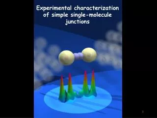
Single-molecule electronic properties Electron transfer (chemistry) Conduction (physics) Many techniques and measurements over the last decade. Cui et al., Science 294, 571 (2001). Dadosh et al., Nature 436, 677 (2005). Liang et al., Nature 417, 725 (2002). Champagne et al., NL 5, 305 (2005). Why is this interesting? • Transport through discrete quantum states • Fundamental physical chemistry problems, novel spectroscopies, potential sensor applications • Tunable model systems for strongly correlated materials • Relevant to any molecular-scale electronics.
“Hot” electrons in the metal leads. • Electronic transitions in the molecule • Chemical reactions Quantum transport: A complicated, nonequilibrium problem! Apply bias…. • Molecular vibrations. • Vibrations in the electrodes. • Quantum entanglement.
Quantum transport: A complicated, nonequilibrium problem! • “Hot” electrons in the metal leads. • Electronic transitions in the molecule • Chemical reactions Apply bias…. • Molecular vibrations. • Vibrations in the electrodes. • Quantum entanglement.
Quantum transport: A complicated, nonequilibrium problem! Apply bias…. Big questions: • How important are electron-electron interactions and quantum coherence effects? • How does dissipation work at these scales?
Nonequilibrium, beyond conductance: “shot” noise Conductance: tells us average current under certain voltage bias. If charge was continuous, that would be the end of the story. However, charge comes in discrete lumps…. Theorist fantasy: ordered list of arrival times for each electron. 16:07:23.0000315 16:07:23.0000319 16:07:23.0000371 16:07:23.0000389 16:07:23.0000400 16:07:23.0000422 16:07:23.0000430 16:07:23.0000463 . . . Now we can compute á I ñ, as before, as well as á (I – á I ñ )2ñ (within some bandwidth)
Shot noise http://www.geocities.com/bioelectrochemistry/schottky.htm Classical: Schottky (1918) Noninteracting electrons Arrivals as Poisson process. What if e- arrivals are not independent? More generally: F º Fano factor
Shot noise SI F ~ 2 F ~1 4kBT F ~0 R I • Fano factor tells you about correlations between electron arrivals. • e.g., F = 2 for Poissonian arrival of pairs, as in SC tunnel junction. • In this sense, F tells you about effective charge of excitations. • F → 0 in macroscopic systems at moderate temperatures – inelastic scattering effectively smears out the conductance channels.
Shot noise – quantum case ti = (Quantum) transmission probability through junction T = 0 T¹ 0 If conductance quantization really comes from Landauer physics, expect suppression of noise whenever ti~ 1.
Shot noise suppression Painful, laborious, low freq. measurements, 4.2 K. Shot noise suppression is observed! van den Brom and van Ruitenbeek, PRL 82, 1526 (1999)
Room temperature shot noise measurements • Break junction setup (Nick King, Jeff Russom senior theses) • High-frequency detection method – fast! • Lock-in approach: only look at V-driven noise.
(a) sync sync (b)
Room temperature shot noise measurements • Au contacts, room temperature, acquisition time = hours, V ~ 100 mV • Noise suppression clearly observed! • Tells us that inelastic suppression still not taking place.
How we make single-molecule devices Electromigration technique Park et al., APL75, 301 (1999) current pulse • Analogous to STM: • Conduction dominated by tunneling volume ~ 1 molecule. • Every device is different! • Can’t “see” what’s going on! • Vibrational fingerprint?
Vibrational resonances Drain Source 35 meV Vibrational effects One molecule-specific feature: E
Vibrational resonances Drain Source 35 meV Vibrational effects One molecule-specific feature: E C60 device, 4.2 K Ward et al., J. Phys: Cond. Matt. 20, 374118 (2008)
Vibrational effects Vibrational resonances Drain Source One molecule-specific feature: E Qiu et al., PRL 92, 206102 (2004)
Raman spectroscopy E1 • Inelastic light scattering. • Requires a = a(r). • Time-varying r from vibrations (w0) leads to sum + difference frequency generation with incident light (w). E0 Stokes anti-Stokes Rayleigh • Cross sections typically 10-29 cm2 - very small! • Stokes/anti-Stokes ratio can tell you temperature due to Boltzmann occupancy factor.
Plasmons and surface-enhancement Plasmons = sound waves in the electron fluid. metal nanoparticle
Plasmons and surface-enhancement Plasmons = sound waves in the electron fluid. metal nanoparticle
Plasmons and surface-enhancement Plasmons = sound waves in the electron fluid. metal nanoparticle
Plasmons and surface-enhancement Plasmons = sound waves in the electron fluid. metal nanoparticle
Plasmons and surface-enhancement Plasmons = sound waves in the electron fluid. metal nanoparticle dimer
Plasmons and surface-enhancement Plasmons = sound waves in the electron fluid. metal nanoparticle dimer • Local electric field can be much larger (g(w)) than incident field! • Raman scattering rate ~ g(w)2g(w’)2 • If g(w), g(w’) ~ 1000 each, then Raman enhanced by 1012. • Single-molecule sensitivity possible in surface-enhanced Raman spectroscopy (SERS).
1 µm Vibrational Spectroscopy 50 µm Nanoscale gaps are ideal for surface-enhanced Raman spectroscopy.
Vibrational Spectroscopy Si • EM calculations (FDTD) show that nanometer-scale protrusions can lead readily to SERS enhancements approaching 1012 (!).
Vibrational Spectroscopy • At nanogap, large SERS signal, “blinking”, and spectral diffusion. • Simultaneous transport + Raman would open many possibilities.
Vibrational Spectroscopy A B C 1 µm D E Remember, data so far taken in air, at room temperature.
Transport + SERS • Enhancement “turns on” as junction is migrated. • Inter-electrode plasmon modes form once conductance ~ 10-4 S.
Transport + SERS • Raman and transport correlate very strongly in time. • Demonstrates single-molecule Raman sensitivity. • Demonstrates multifunctional sensing at single-molecule level.
Simultaneous conduction + SERS D. Ward et al., J. Phys. Condens. Matt. 20, 374118 (2008).
Stokes-AntiStokes and local temperature • Ratio of antiStokes to Stokes intensities provides a measure of excited state population, and therefore effective temperature. • The exponential makes things challenging. Ignoring cross-section and enhancement issues, 450 cm-1 mode at 80 K → AS/S = 3.8 × 10⁻⁴. So, 10000 Stokes counts → 3.8 antiStokes counts • SERS itself can lead to optical pumping of excited state. Can we see bias-driven effects?
1625 1/cm 1317 1/cm
50 mV A Upper bound on temperature at A is ~220 K
500 mV D B F? C A E D E F B A C A=560 K B=520 K C=508 K D=513 K E=470 K F=382 K
Conclusions • We can make atomic- and molecular-scale structures and measure their electronic and optical properties. • We can see quantum effects in electronic conduction at room temperature in these gadgets. • We can make nanoscale optical antennas that allow chemical sensing and vibrational pumping at the single-molecule level. • Basic science with potential applications in sensing, photonics, cutting-edge nanoelectronics. Very exciting! We have a lot to do….
Acknowledgments My group: Daniel Ward, Jeff Worne, Alexandra Fursina, Patrick Wheeler, Kenneth Evans, Amanda Whaley,Ruoyu Chen, HengJi, Dr. Gavin Scott, Dr. Jiang Wei Collaborators: J.M. Tour, N.J. Halas, P. Nordlander, J. C. Cuevas D. Ward et al., NanoLett. 7, 1396-1400 (2007). D. Ward et al., NanoLett. 8, 919-924 (2008). D. Ward et al., J. Phys. Condens. Mat.20, 374118 (2008). P. J. Wheeler et al.,NanoLett. 10, 1287-1292(2010).
Large aspect ratio nanogaps by self-alignment II. Oxidation I. E-beam lithography First electrode CrxOy Cr IV. Etching away Cr/Cr2O3 layer Room temperature, 90 sec, Cr-7 etchant III. Second electrode A. Fursina et al., Appl. Phys. Lett. 93, 113102 (2008)
Uniquenanofab capabilities Industrially scalable nanogap fabrication method 20 μm
Optical rectification Tunneling nonlinearity can lead to DC current from AC bias. Light induces some Vopt across our gap, oscillating at ~ 1015 Hz. Rectification (photocurrent) can lead to a means of quantitatively estimating the field enhancement factor! (provided that tunneling is fast!)
Optical rectification This has been shown to work quantitatively at microwave frequencies.
Validity of classical rectification In general, correct quantum treatment = photon-assisted tunneling. Tien-Gordon (perturbative) approach: First order in alpha: If a << 1 and nonlinearity varies little (i.e., DOS is “boring”) over then classical rectification picture is reasonable. J. C. Cuevas
Validity of classical rectification Viljas and Cuevas, PRB 75, 075406 (2007) DFT calculations originally done for Au contacts show that we are likely in luck as far as DOS goes, as long as junctions are clean.
Optical rectification How would this work? • Use low freq measurement (wlow = 2p´ 2 kHz) with known Vac , and use lock-in at 2wlow to measure (d2I/dV2) as a function of Vdc. • Simultaneously, measure the photocurrent as a function of Vdc (use a second lock-in and chop the light). • Adjust Vac until the two signals (2nd harmonic + photocurrent) are identical. Voila – Vac should now = Vopt. d2I/dV2 I V V
Actual experiment: • Apply dc + small ac voltage, V0. • Simultaneously measure I, dI/dV, (1/4)d2I/dV2Vo2, and Iphoto as a function of Vdc.
Challenges: • Junction stability when illuminated is comparatively worse. • Capacitance in cryostat wiring makes low freq measurement not as sensitive as we would prefer. • Issues w/ oxide under large bond pads (two distinct problems: mismatch of conductance and d2I/dV2; and/or no spatial dependence of photocurrent).
Examples: dI/dV in units of nA/V. Quantitative agreement between Iphotoand (1/4)d2I/dV2 V02 happens when V0 = 30 mV. This implies Vac from the optical field is ~ 30 mV! Measured dI/dV at Vdc = 0 implies an interelectrode gap of ~ 0.14 nm, implying local field = 2.1 x 10⁸ V/m. Incident intensity = 22.6 kW/cm2 Implied field enhancement ~ 718x