ELEKTRONIKA DASAR
110 likes | 695 Vues
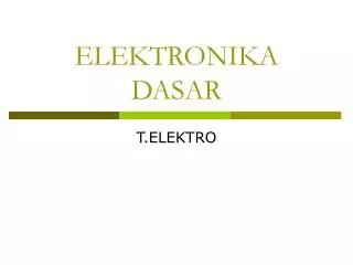
ELEKTRONIKA DASAR. T.ELEKTRO. Heavily doped. E. C. E. C. n. p. p. n. p. n. B. B. TRANSISTOR : Bipolar Junction Transistor. Konstruksi Transistor adalah piranti semikonduktor tiga terminal yang dibangun dari : dua material tipe p dan satu material tipe n, atau

ELEKTRONIKA DASAR
E N D
Presentation Transcript
ELEKTRONIKA DASAR T.ELEKTRO
Heavily doped E C E C n p p n p n B B TRANSISTOR : Bipolar Junction Transistor • Konstruksi Transistor adalah piranti semikonduktor tiga terminal yang dibangun dari : • dua material tipe p dan satu material tipe n, atau • dua material tipe n dan satu material tipe p.
Heavily doped E C E C n p p n p n B B BJT Doping pada bagian tengah diberikan lebih sedikit dibandingkan dengan bagian luar (sekitar 10:1). Doping rendah ini mengurangi konduktiviti material dengan membatasi jumlah elektron bebas. Istilah bipolar berasal dari kenyataan bahwa elektron dan holes berpartisipasi dalam proses pembangkitan arus.
BJT : Operasi Transistor • Transistor beroperasi dengan memberikan bias pada kedua junction. Bias maju pada junction BE menyebabkan sejumlah besar majority carrier (holes) yang terhubung ke terminal emitter terdifusi melewati junction menuju materi tipe n (basis). Karena ketersediaan elektron bebas pada materi tipe n lebih sedikit dari hole yang terdifusi, hanya sedikit holes yang ber-kombinasi dengan elektron dan menghasilkan arus pada terminal basis. • Sebagian besar hole akan begerak melewati depletion region pada junction base-collector (junction base-collector di-bias mundur) dan keluar pada terminal collector.
BJT • Total arus dari terminal emitter sama dengan arus pada terminal collector ditambah arus pada terminal basis. • IE = IC + IB • Arus collector IC terdiri dari dua komponen, yang berasal dari majority carrier dan minority carrier. Arus dari minority carrier disebut dengan ICO (arus collector dengan terminal emitter open). • IC =ICmajority +ICO • ICO bernilai sangat kecil dan umumnya bisa diabaikan
BJT • Tegangan base-emitter (VBE) bisa dianggap sebagai variabel pengontrol dalam menentukan operasi transistor. Arus collector dikaitkan dengan tegangan VBE (Ebers-Moll / Shockley equation): • Arus collector IC proporsional terhadap arus IB dengan hubungan: • IC = IB • IC = IE
BJT • Data spesifikasi transistor (dari pabrik) di-set nilai maksimum yang tidak boleh dilampaui dalam operasi. Spesifikasi ini memberi batasan operasi transistor dalam rangkaian. • Contoh spesifikasi transistor silikon 2N2222 • Collector-Base Voltage = 60 v • Collector-Emitter Voltage = 30 v • Base-Emitter Voltage = 5 v • Power dissipation = 500 mW • Temperature 125 C
BJT : Konfigurasi • Common Base Arah arus yang ditunjukkan adalah arah arus konvensional ( sesuai pergerakan holes) • Daerah operasi: • Cut-off • Aktif • saturasi
Common-base • Penguatan