Impact of Boron Doping on Carbon Nanotubes: Electronic and Structural Effects
Boron doping in carbon nanotubes alters the electronic profiles by creating acceptor states near the valence band edge, increasing conductance, and modifying electron hopping magnitude. The electrical properties are influenced by the competition between scattering density and hole carrier increase. The temporary formation of sp3 bonds upon bending reduces resistance. This study explores the effects of boron doping on the structure and electronic behavior of carbon nanotubes, shedding light on their potential for semiconductor applications.

Impact of Boron Doping on Carbon Nanotubes: Electronic and Structural Effects
E N D
Presentation Transcript
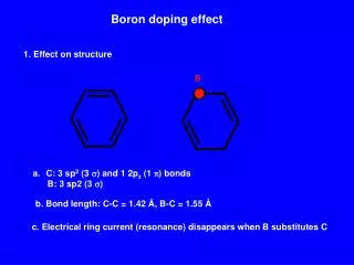
Boron doping effect 1. Effect on structure B • C: 3 sp2 (3 ) and 1 2pz(1 ) bonds • B: 3 sp2 (3 ) b. Bond length: C-C = 1.42 Å, B-C = 1.55 Å c. Electrical ring current (resonance) disappears when B substitutes C
CB metallic EF VB CB Eg EF VB Semiconductor 2. Effect on electronic profile CNT
CB * EF VB Free electronic-like (metallic) BC3 tube
2. Effect on electronic profiles CB metallic EF VB EF depression to VB edge more than 2 sub-bands crossing at EF i.e. conductance increases CB Eg EF BC3 state (acceptor) New Eg Random doping of B in CNT VB Semiconductor Eg reduction by EF depression
B-doping • EF depression Eg reduction (semiconductor tube) and number of conduction • channel increase (conductance > 4e2/h, metallic tube). b. Creation of acceptor state near to VB edgeand increase in hole carrier density (11016 spins/g for CNTs, 61016 spins/g for BCNTs). c. Electron scattering density increase by B-doping centers (i.e. shorter mean free path and relaxation time compared with CNTs, = 0.4 ps and 4-10 ps for BCNTs and CNTs) d. The actual conductivity depends on competition between scattering density and increase in hole carrier (in practice, the latter > the former, so conductance ) scattering B+ e-
e. Electron hopping magnitude in -band increase Overlap of -electron wave function hopping e- -band (CB) -band (VB) -band (CB) B dopant BC3 state
f. Less influence on conductivity upon strain application For CNT R Deflection angle
Resistance reduction is due to (i) temporary formation of sp3 at bend region and (ii) increasing hopping magnitude upon bending Temporary formation of sp3 character upon bending bending Planar sp2 Tetrahedral sp3
-band planar -band -band e- hopping bending
For BCNTs -band is blocked by bending -band BC3-state is less affected by bending, so channel remains opened for conduction. (note that tube bending induced distortion only occurs in -wave function and valence band essentially remains intact, if, only if, distortion also takes place in valence band the tube fracture occurs)