ERD Memory Discussion
ERD Memory Discussion. Victor Zhirnov July 10, 2011 San Francisco, CA. Outline. ERD Memory Tables/Text Updates Memory Select Device Section Storage Class Memory Section. ERD Memory Tables. 2011 Memory Transition Table. 2011 ERD Memory Table. Emerging Ferroelectric Memory.

ERD Memory Discussion
E N D
Presentation Transcript
ERD Memory Discussion Victor Zhirnov July 10, 2011 San Francisco, CA
Outline • ERD Memory Tables/Text Updates • Memory Select Device Section • Storage Class Memory Section
Emerging Ferroelectric Memory • Combines two subcategories: • Ferroelectric FET • Ferroelectric tunnel junction • Should not be confused with conventional ferroelectric memory or FeRAM • Based on FE capacitor • Is currently in PIDS • Temporary working name: • Emerging Ferroelectric Memory • Suggestions are welcome
Emerging Ferroelectric Memory • Text update: completed • Table ERD5 update: Work in progress • References update: Work in progress
Nanomechanical Memory • Text update: completed • De-emphasized CNT-based nanomechanical memory (earlier Nantero concept) • Table ERD5 update: Work in progress • References update: Work in progress
RedOx Memory • Replaces former nanothermal and Ionic memory categories • New text based on the materials from Barsa Workshop (white papers and presentations) • Numbers in Table ERD5 updated • References update: Work in progress
Macromolecular Memory • Text update: Work in progress • Table ERD5 update: Work in progress • References update: Work in progress
Molecular Memory • Text update: Work in progress • Table ERD5 update: Work in progress • References update: Work in progress
Input Received Alex Bratkovski (HP) Curt Richter (NIST) Eric Pop (U Illinois) An Chen (GLOBALFOUNDRIES) Rainer Waser (U Aachen) Hiro Akinaga (AIST) Table ERD5/Redox Memory Table ERD5/Redox Memory Table ERD4/PCM Table ERD5/Mott Memory Text / References Text / References
Memory Select Device Wei Lu (U Michigan)An Chen (GLOBALFND) Dirk Wouters (IMEC) Kwok Ng (SRC)Victor Zhirnov (SRC)
Memory Select Device TWG: Wei Lu (U Michigan)An Chen (GLOBALFND) Dirk Wouters (IMEC) Kwok Ng (SRC)Victor Zhirnov (SRC) The fundamental study team Rainer Waser (U Aachen) Thomas Vogelsang (RAMBUS) Zoran Krivokapic(GLOBALFND) Al Fazio (Intel) Kyu Min (Intel) U-In Chung (Samsung) Matthew Marinella (Sandia Labs)
Memory Select Device: Intro • A memory cell in array can be viewed as being composed of two fundamental components: the ‘Storage node’, and the ‘Select device’ to minimize sneak current through unselected cells. • Both components impact scaling limits for memory. • Several advanced concepts of resistance-based memories offer storage node scaling down below 10 nm, and the memory density will be limited by the select device. • The select device thus represents a serious bottleneck for memory scaling to 10 nm and beyond.
Planar FET select device (8-9)F2 L. Li, K. Lu, B. Rajendran, T. D. Happ, H-L. Lung, C. Lam, and M. Chan, “Driving Device Comparison for Phase-Change Memory”, IEEE Trans. Electron. Dev. 58 (2011) 664-671
Vertical Select Devices Vertical diode Vertical FET L. Li, K. Lu, B. Rajendran, T. D. Happ, H-L. Lung, C. Lam, and M. Chan, “Driving Device Comparison for Phase-Change Memory”, IEEE Trans. Electron. Dev. 58 (2011) 664-671
Vertical Select Devices Vertical diode 4F2 Vertical FET 5.3F2
Vertical Transistor Select Devices Experimental demonstrations of vertical transistors in memory arrays. * projected cell size **has potential as a select device (not demonstrated)
I V Two-terminal selector devices • External 2-terminal structure with non-linear characteristics • e.g. switching diode-type behavior for unipolar memory cells • for bipolar cells, selectors with two-way switching behavior are needed, e.g. Zener diode, avalanche diode etc. • Storage element with inherent rectifying/isolation properties ION1 ON2 ION OFF ON1 OFF unipolar bipolar
Benchmark Select Device Parameters *ON/OFF current ratio at ~(1V) supply **Proposed alternative schemes of array biasing could result in relaxed requirements on the select device ON/OFF ratio [5]
Diode-type Select Devices • pn-diode, • Schottky diode • Heterojunction diode • BARITT diode • Zener diode • Reverse breakdown Schottky diode Unipolar cell Bipolar cell
Switch-type select devices • Innovative device concepts that exhibit resistive switching behavior. • In some of these concepts the device structure/physics of operation is similar to the structure of the storage node. • A modified memory element could act as select device! • a ‘nonvolatile’ switch is required for the storage node, while for select device depending on the approaches non-volatility may not be necessary and can sometimes be detrimental. • Knowledge gained from studying new memory phenomena can be used for select device!
Resistive-Switch-type select devices I • Mott-transition switch • is based on the Mott Metal-Insulator transition • a volatile resistive switch, • A VO2-based Mott-transition device has been demonstrated as a selection device for NiOx RRAM element [Ref: M.J. Lee, “Two Series Oxide Resistors Applicable to High Speed and High Density Nonvolatile Memory,” Adv. Mater. 19, 3919 (2007).]. • The feasibility of the Mott-transition switch as selection devices still needs further research. • Threshold switch • is based the threshold switching in MIM structures caused by electronic charge injection/trapping • Significant resistance reduction can occur at a threshold voltage and this low-resistance state quickly recovers to the original high-resistance state when the applied voltage falls below a holding voltage.
Resistive-Switch-type select devices II • MIEC switch • observed in materials that conduct both ions and electronic charges – so called mixed ionic electronic conduction materials (MIEC). • The resistive switching mechanism is similar to the ionic memories. • Complementary resistive switch • the memory cell is composed of two identical non-volatile ReRAM switches connected back-to-back. • Example: Pt/GeSe/Cu/GeSe/Pt structure • During idle conditions one of the ReRAM switch is off so sneak current is reduced. • Read involves turning on both ReRAM devices and is destructive.
Mott-Switch as Select Device Combined device switching Threshold Switching Resistive Switching Lee 2007 - demonstrated very fast writing and erasing process, 1.5V; 10ns. - read operation at 0.6V also doesn’t seem to be degraded by switch element - on/off ratio ~ 103, Ion ~ 400 A/cm2
Threshold switch as Select Device VReset Current VSet Current Vread Voltage Voltage Schematic I-V characteristics of threshold switch Schematic I-V characteristics of combined unipolar RRAM devices with threshold switch as the select device -Similar to Mott switch, but not restricted by the transition temperature - Organic Threshold Switch as select device integrated with PCM (Kau 2009) - 9ns switching speed and 106 endurance demonstrated - Array data not available. Arrays based on MOS select devices presented
MIEC-Switch as Select Device Switch device characteristics Gopalakrishnan 2010 - MIEC switching due to redistribution of Cu ions and associated hole diff. current - Current scales with BEC area. Needs very thin (~ 13nm) dielectric for high current - Combined MIEC/PCM device demonstrated with endurance of > 3x10⁴ cycles.
Complementary ReRAM cell Two identical RRAM devices connected back-to-back (1,1) C-ReRAM 0 = (0,1) C-ReRAM 1 = (1,0) Waser 2010 (1,0) (1,0) (0,1) (0,1) VT,set<Vread<2VT,reset Vc,reset (1,1) (1,0) -> (1,1), -> high read current (0,1) -> (0,1), -> low read current Vc,set Vread
Complementary ReRAM cell CRRAM cell C-ReRAM based on back-to-back Pt/ZrOx/HfOx/BE devices Read endurance is limited to 105 Lee 2010
Resistive-Switch-type select devices Source: Philip Wong / Stanford
Fundamental Issues • For scaled diode-type select devices two fundamental challenges are: • Contact resistance • Lateral depletion effects • Very high concentration of dopants are needed to minimize both effects. • high dopant concentrations result in increase reverse currents in classical diode structures and therefore in reduced ON/OFF ratio. • For switch-type select devices the main challenges are: • identifying the right material • and the switching mechanism to achieve the required drive current density, ON/OFF ratio and reliability.
Selection Devices Summary • Experimental two-terminal select devices have yet to meet the benchmark specifications • Hence, outstanding research issues persist • 2011 MSD tables and text reflects both target parameters and experimental status • More detailed benchmarking and further analysis is currently underway • Currently no data from functional arrays based on two-terminal select devices are available
SCM Team: Barry Schechtman (INSIC)Rod Bowman (Seagate)Geoff Burr (IBM)Bob Fontana (IBM)Michele Franceschini (IBM) Rich Freitas (IBM)Kevin Gomez (Seagate)Mark Kryder (CMU)Antoine Khroueir (Seagate)Kroum Stoev (Western Digital)Winfried Wilcke (IBM) Thomas Vogelsang (RAMBUS) Matthew Marinella (Sandia Labs)Jim Hutchby (SRC)Victor Zhirnov (SRC)
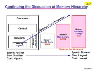
Storage-class memory (SCM) • Research and development efforts are underway worldwide on several nonvolatile memory technologies that not only complement the existing memory but also reduce the distinction between memory and storage1 • Memory: fast, evanescent, random-access, expensive • Storage: slow, permanent, sequential-access, inexpensive • Storage-class memory (SCM): Emerging solid-state technologies with (some) attributes of both memory and storage devices • May eventually replace discs and (perhaps) DRAM1 1 “Storage-class memory: The next storage system technology”, by R. F. Freitas and W. W. Wilcke, IBM J. Res. & Dev. 52 (2008) 439
Draft Section on SCM is Completed • Storage-class memory (SCM) describes a device category that combines the benefits of solid-state memory, such as high performance and robustness, with the archival capabilities and low cost of conventional hard-disk magnetic storage. • Such a device requires a nonvolatile memory technology that could be manufactured at a very low cost per bit. • As the scalability of flash is approaching its limit, emerging technologies for non-volatile memories need to be investigated for a potential “take over” of the scaling roadmap for flash. • In principle, such new SCM technology could engender two entirely new and distinct levels within the memory and storage hierarchy, located below off-chip DRAM and above mechanical storage, and differentiated from each other by access time.
Hard-disk Drive • Conventionally, magnetic hard-disk drives are used for nonvolatile data storage. • The cost of HDD storage (in $/GB) is extremely low and continues to decrease. • Issues: • poor random access time • relatively high energy consumption, • large form factor, • limited reliability.
Flash memory: Device Challenges • NAND flash has recently become an alternative storage technology • faster access times, • smaller size and potentially lower energy consumption, as compared to HDD. • The NAND-based solid state drive (SSD) market has flourished recently. • There are several serious limitations of NAND flash for storage applications • poor endurance (104 – 105 erase cycles), • modest retention (typically 10 years on the new device, but only 1 year at the end of rated endurance lifetime), • long erase time (~ms), and high operation voltage (~15V).
Flash SSD: Architectural Challenges • Page/block-based architecture, • doesn’t allow for a direct overwrite of data, • requiring sophisticated garbage collection • bulk erase procedures, • Computation-intensive data management • Takes extra memory space, • Limits performance • Accelerates the wearing out of memory cells. • Lower power potential compromised in current SSD implementations
Flash Scaling Challenges • Flash memory scaling doesn’t improve (and sometimes degrades) the basic performance characteristics • read, write and erase latencies have been nearly constant for over a decade • Extreme scaling results in the degradation of retention time and endurance, • critical for storage applications! • There are opportunities for prototypical and emerging memory technologies to enter the non-volatile solid state memory space.
Prototypical and emerging memory technologies for SCM applications • As the scalability of flash is approaching its limit, emerging technologies for non-volatile memories need to be investigated for a potential “take over” of the scaling roadmap for flash. • It appears that storage applications could be the primary driver for the new memory technologies, • may help to overcome the fundamental shortcomings of flash technology. • In principle, such new SCM technology could engender two entirely new and distinct levels within the memory and storage hierarchy, located below off-chip DRAM and above mechanical storage, which are differentiated from each other by access time.
I. S-type storage-class memory • The first new level, identified as S-type storage-class memory (S-SCM), would serve as a high-performance solid-state drive • accessed by the system I/O controller much like an HDD. • S-SCM would need to provide at least the same data retention as flash, • offering new direct overwrite and random access capabilities (which can lead to improved performance and simpler systems) • However, it would be absolutely critical that the device cost for S-SCM be no more than 1.5-2x(1-1.5x? IN THE MATURE STATE)) higher than NAND flash • If the cost per bit could be driven low enough through ultrahigh memory density, ultimately such an S-SCM device could potentially replace magnetic hard-disk drives in enterprise storage server systems.
II. M-type storage-class memory • M-SCM: • should offer a read/write latency of less than 1 ms. • would allow it to remain synchronous with a memory system, allowing direct connection from a memory controller and bypassing the inefficiencies of access through the I/O controller. • Would be to augment a small amount of DRAM to provide the same overall system performance as a DRAM-only system, while providing • Moderate retention, • Lower power-per-GB and lower cost-per-GB than DRAM. • Endurance is particularly critical • the time available for wear-leveling, error-correction, and other similar techniques is limited • > 109 cycles
Target device and system specifications for SCM * enterprise class **single-level cell (SLC)
Prototypical and emerging memory technologies for SCM applications • Necessary attributes of a memory device for the storage-class memory applications are: • Scalability • Multilevel Cell - MLC (MLC vs extreme scaling dilemma) • 3D integration (stacking) • Fabrications costs • Endurance (for M-SCM) • Retention (for S-SCM) • The driving issue is to minimize the cost per bit
Potential of the current prototypical research memory candidates for SCM applications A likely introduction of these new memory devices to the market is by the hybridsolid-state discs, where the new memory technology complements the traditional flash memory to boost the SSD performance. Experimental implementations of FeRAM/flash and PCRAM/flash have recently been explored. It was shown that the PCRAM/Flash hybrid improves SSD operations by decreasing the energy consumption and increasing the lifetime of flash memory.

