Download

1 / 66
680 likes | 1.23k Vues
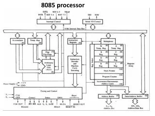
8085 PROCESSOR UNIT I Mr. S. VINOD ASSISTANT PROFESSOR EEE DEPARTMENT. 8085 PROCESSOR. --Functional block diagram --Signals --Memory interfacing --I/O ports and data transfer concepts --Timing Diagram --Interrupt structure. Pin detail of 8085.

E N D
8085 PROCESSOR UNIT I Mr. S. VINOD ASSISTANT PROFESSOR EEE DEPARTMENT
8085 PROCESSOR --Functional block diagram --Signals --Memory interfacing --I/O ports and data transfer concepts --Timing Diagram --Interrupt structure.
The 8085 Microprocessor Architecture • The 8085 is an 8-bit general purpose microprocessor that can address 64K Byte of memory. • It has 40 pins and uses +5V for power. It can run at a maximum frequency of 3 MHz. • The pins on the chip can be grouped into 6 groups: • Address Bus. • Data Bus. • Control and Status Signals. • Power supply and frequency. • Externally Initiated Signals. • Serial I/O ports.
The Address and Data Busses • The address bus has 8 signal lines A8 – A15 which are unidirectional. • The other 8 address bits are multiplexed (time shared) with the 8 data bits. • So, the bits AD0 – AD7 are bi-directional and serve as A0 – A7 and D0 – D7 at the same time. • During the execution of the instruction, these lines carry the address bits during the early part, then during the late parts of the execution, they carry the 8 data bits. • In order to separate the address from the data, we can use a latch to save the value before the function of the bits changes.
The Control and Status Signals • There are 4 main control and status signals. These are: • ALE: Address Latch Enable. This signal is a pulse that become 1 when the AD0 – AD7 lines have an address on them. It becomes 0 after that. This signal can be used to enable a latch to save the address bits from the AD lines. • RD: Read. Active low. • WR: Write. Active low. • IO/M: This signal specifies whether the operation is a memory operation (IO/M=0) or an I/O operation (IO/M=1). • S1 and S0 : Status signals to specify the kind of operation being performed .Usually un-used in small systems.
Frequency Control Signals • There are 3 important pins in the frequency control group. • X0 and X1 are the inputs from the crystal or clock generating circuit. • The frequency is internally divided by 2. • So, to run the microprocessor at 3 MHz, a clock running at 6 MHz should be connected to the X0 and X1 pins. • CLK (OUT): An output clock pin to drive the clock of the rest of the system. • We will discuss the rest of the control signals as we get to them.
The ALU • In addition to the arithmetic & logic circuits, the ALU includes the accumulator, which is part of every arithmetic & logic operation. • Also, the ALU includes a temporary register used for holding data temporarily during the execution of the operation. This temporary register is not accessible by the programmer.
The Flags register • There is also the flags register whose bits are affected by the arithmetic & logic operations. • S-sign flag • The sign flag is set if bit D7 of the accumulator is set after an arithmetic or logic operation. • Z-zero flag • Set if the result of the ALU operation is 0. Otherwise is reset. This flag is affected by operations on the accumulator as well as other registers. (DCR B). • AC-Auxiliary Carry • This flag is set when a carry is generated from bit D3 and passed to D4 . This flag is used only internally for BCD operations. (Section 10.5 describes BCD addition including the DAA instruction). • P-Parity flag • After an ALU operation if the result has an even # of 1’s the p-flag is set. Otherwise it is cleared. So, the flag can be used to indicate even parity. • CY-carry flag • Discussed earlier
8085 Instruction Set The 8085 instructions can be classified as follows: • Data transfer operations • Arithmetic operations (ADD, SUB, INR, DCR) • Logic operations • Branching operations (JMP, CALL, RET) • Between registers • Between memory location and a register • Direct write to a register / memory • Between I/O device and accumulator
Simple Data Transfer Operations Examples: • MOV B,A 47 From ACC to REG • MOV C,D 4A Between two REGs • MVI D,47 16 Direct-write into REG D 47
Simple Data Transfer Operations Example: • OUT 05 D3 05 Contents of ACC sent to output port number 05.
Branching Operations Note: This is an unconditional jump operation. It will always force the program counter to a fixed memory address continuous loop !
Branching Operations Conditional jump operations are very useful for decision making during the execution of the program.
Data transfer operation • LHLD Load H & L Registers Directly from Memory • SHLD Store H & L Registers Directly in Memory • LXI Load Register Pair with Immediate data • LDAX Load Accumulator from Address in Register Pair • STAX Store Accumulator in Address in Register Pair • XCHG Exchange H & L with D & E • XTHL Exchange Top of Stack with H & L
Arithmetic Operations • ADC Add to Accumulator Using Carry Flag • ACI Add Immediate data to Accumulator Using Carry • SBB Subtract from Accumulator Using Borrow (Carry) Flag • SBI Subtract Immediate from Accumulator Using Borrow (Carry) Flag • INX Increment Register Pair by One • DCX Decrement Register Pair by One • DAD Double Register Add; Add Content of Register Pair to H & L Register Pair
Logic Operations The Compare instructions compare the content of an 8-bit value with the contents of the accumulator • CMP Compare • CPI Compare Using Immediate Data The rotate instructions shift the contents of the accumulator one bit position to the left or right: • RLC Rotate Accumulator Left • RRC Rotate Accumulator Right • RAL Rotate Left Through Carry • RAR Rotate Right Through Carry Complement and carry flag instructions: • CMA Complement Accumulator • CMC Complement Carry Flag • STC Set Carry Flag
Branching Operations the conditional branching instructions are specified as follows: Jumps Calls Returns C CC RC (Carry) INC CNC RNC (No Carry) JZ CZ RZ (Zero) JNZ CNZ RNZ (Not Zero) JP CP RP (Plus) JM CM RM (Minus) JPE CPE RPE (Parity Even) JP0 CPO RPO (Parity Odd) Two other instructions can affect a branch by replacing the contents or the program counter: PCHL Move H & L to Program Counter RST Special Restart Instruction Used with Interrupts
Stack I/O and Machine Control Instructions The following instructions affect the Stack and/or Stack Pointer: PUSH Push Two bytes of Data onto the Stack POP Pop Two Bytes of Data off the Stack XTHL Exchange Top of Stack with H & L SPHL Move content of H & L to Stack Pointer The Machine Control instructions are as follows: EI Enable Interrupt System DI Disable Interrupt System HLT Halt NOP No Operation
TIMING DIAGRAM Timing Diagram is a graphical representation. It represents the execution time taken by each instruction in a graphical format. The execution time is represented in T-states. Instruction Cycle: The time required to execute an instruction is called instruction cycle. Machine Cycle: The time required to access the memory or input/output devices is called machine cycle. T-State: The machine cycle and instruction cycle takes multiple clock periods. A portion of an operation carried out in one system clock period is called as T-state.
MACHINE CYCLES OF 8085 The 8085 microprocessor has 5 (seven) basic machine cycles. • Opcode fetch cycle (4T) • Memory read cycle (3 T) • Memory write cycle (3 T) • I/O read cycle (3 T) • I/O write cycle (3 T)
Memory Write Machine Cycle • The memory write machine cycle is executed by the processor to write a data byte in a memory location. • The processor takes, 3T states to execute this machine cycle.
I/O Write Cycle • The I/O write machine cycle is executed by the processor to write a data byte in the I/O port or to a peripheral, which is I/O, mapped in the system. • The processor takes, 3T states to execute this machine cycle
Timing diagram for STA 526AH • STA means Store Accumulator -The contents of the accumulator is stored in the specified address(526A). • The opcode of the STA instruction is said to be 32H. It is fetched from the memory 41FFH(see fig). - OF machine cycle • Then the lower order memory address is read(6A). - Memory Read Machine Cycle • Read the higher order memory address (52).- Memory Read Machine Cycle • The combination of both the addresses are considered and the content from accumulator is written in 526A. - Memory Write Machine Cycle • Assume the memory address for the instruction and let the content of accumulator is C7H. So, C7H from accumulator is now stored in 526A.
Timing diagram for IN C0H • Fetching the Opcode DBH from the memory 4125H. • Read the port address C0H from 4126H. • Read the content of port C0H and send it to the accumulator. • Let the content of port is 5EH.
INTERRUPT STRUCTURE • Interrupt is signals send by an external device to the processor, to request the processor to perform a particular task or work. • Mainly in the microprocessor based system the interrupts are used for data transfer between the peripheral and the microprocessor. • The processor will check the interrupts always at the 2nd T-state of last machine cycle. • If there is any interrupt it accept the interrupt and send the INTA (active low) signal to the peripheral. • The vectored address of particular interrupt is stored in program counter. • The processor executes an interrupt service routine (ISR) addressed in program counter. • It returned to main program by RET instruction.
TYPES OF INTERRUPTS: It supports two types of interrupts. • Hardware • Software Software interrupts: • The software interrupts are program instructions. These instructions are inserted at desired locations in a program. • The 8085 has eight software interrupts from RST 0 to RST 7. The vector address for these interrupts can be calculated as follows. Interrupt number * 8 = vector address For RST 5 5 * 8 = 40 = 28H Vector address for interrupt RST 5 is 0028H
HARDWARE INTERRUPTS: • An external device initiates the hardware interrupts and placing an appropriate signal at the interrupt pin of the processor. • If the interrupt is accepted then the processor executes an interrupt service routine. • The 8085 has five hardware interrupts (1) TRAP (2) RST 7.5 (3) RST6.5 (4) RST 5.5 (5) INTR
TRAP • This interrupt is a non-maskable interrupt. It is unaffected by any mask or interrupt enable. • TRAP is the highest priority and vectored interrupt. • TRAP interrupt is edge and level triggered. This means hat the TRAP must go high and remain high until it is acknowledged. • In sudden power failure, it executes a ISR and send the data from main memory to backup memory. • The signal, which overrides the TRAP, is HOLD signal. (i.e., If the processor receives HOLD and TRAP at the same time then HOLD is recognized first and then TRAP is recognized). • There are two ways to clear TRAP interrupt. 1.By resetting microprocessor (External signal) 2.By giving a high TRAP ACKNOWLEDGE (Internal signal)
RST 7.5 • The RST 7.5 interrupt is a maskable interrupt. • It has the second highest priority. • It is edge sensitive. ie. Input goes to high and no need to maintain high state until it recognized. • Maskable interrupt. It is disabled by, 1.DI instruction 2.System or processor reset. 3.After reorganization of interrupt.
RST 6.5 and 5.5 • The RST 6.5 and RST 5.5 both are level triggered. • ie. Input goes to high and stay high until it recognized. • Maskable interrupt. It is disabled by, 1.DI, SIM instruction 2.System or processor reset. 3.After reorganization of interrupt. • Enabled by EI instruction. • The RST 6.5 has the third priority whereas RST 5.5 has the fourth priority.
INTR • INTR is a maskable interrupt. It is disabled by, 1.DI, SIM instruction 2.System or processor reset. 3.After reorganization of interrupt. Enabled by EI instruction. • Non- vectored interrupt. After receiving INTA (active low) signal, it has to supply the address of ISR. • It has lowest priority. • It is a level sensitive interrupts. ie. Input goes to high and it is necessary to maintain high state until it recognized. • The following sequence of events occurs when INTR signal goes high. • 1. The 8085 checks the status of INTR signal during execution of each instruction. • 2. If INTR signal is high, then 8085 complete its current instruction and sends active low interrupt acknowledge signal, if the interrupt is enabled • 3. In response to the acknowledge signal, external logic places an instruction OPCODE on the data bus. In the case of multibyte instruction, additional interrupt acknowledge machine cycles are generated by the 8085 to transfer the additional bytes into the microprocessor. • 4. On receiving the instruction, the 8085 save the address of next instruction on stack and execute received instruction.