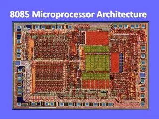
8085 processor
8085 processor. Bus system in microprocessor. Intel 8085 Block Diagram. Intel 8085 Signals. Stored program organization. Basic computer registers and memory. List of Registers for the Basic Computer. Computer Instructions. each computer has its own unique instruction set.

8085 processor
E N D
Presentation Transcript
Computer Instructions each computer has its own unique instruction set. • Instruction types and formats The basic computer has three instruction code formats • Each format has 16 bits. • The operation code (opcode) part of the instruction contains three bits • the meaning of the remaining 13 bits depends on the operation code encountered
A memory-reference instruction • uses 12 bits to specify an address and one bit to specify the addressing mode I. The I bit is • equal to 0 for direct address • 1 for indirect address 2) The register-reference instructions are recognized by the operation code 111 with a 0 in the leftmost bit (bit 15) of the instruction 3) input-output instruction are recognized by the operation code 111 with a 1 in the leftmost bit (bit 15) of the instruction
effective address to be the address of the operand in a computation-type instruction. Thus the effective address in the instruction in memory address 22 is 457 and the effective address in the instruction in memory address 35 in the instruction is 1350.
Instruction Cycle • In the basic computer each instruction cycle consists of the following phases: • Fetch an instruction from memory. • Decode the instruction. • Define the operation. • Read the effective address from memory if the instruction has an indirect address. • Execute the instruction. • read operand or data if any. • execute the specified operation on the data
Fetch and Decode The microoperations for the fetch and decode phases can be specified by the following register transfer statements SC is cleared to 0 T0: AR PC T1: IR M[AR], pc pc+1 T2 : D0,.D7 Decode IR(12-14), I IR(15), AR IR(0-11)
Register-Reference Instructions • Register-reference instructions are recognized by the control when D7 = 1 and I = 0. • These instructions use bits 0 through 11 of the instruction code to specify one of 12 instructions. These 12 bits are available in IR(0-ll). • They were also transferred to AR during time T2
Memory-Reference Instructions Memory-Reference Instructions
BSA: Branch and Save Return Address Example of BSA instruction execution
Timing and Control • The timing for all registers in the basic computer is controlled by a master clock generator. • The clock pulses do not change the state of a register unless the register is enabled by a control signal. • The control signals are generated in the control unit and provide control inputs for : • multiplexers in the common bus, • control inputs in processor registers, and • micro-operations for the accumulator
There are two major types of control organization: • hardwired control and • micro-programmed control • In the HW the control logic is implemented with • gates, flip-flops, decoders, and other digital circuits • In micro., the control information is stored in a control memory. • The control memory is programmed to initiate the required sequence of microoperations
Timing and Control Block Diagram Control unit of basic computer
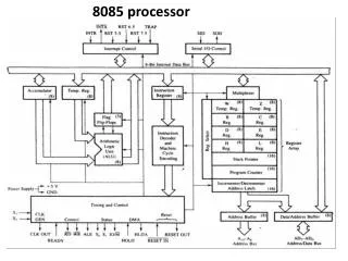
It consists of two decoders, a sequence counter, and a number of control logic gates. An instruction read from memory is placed in the instruction register (IR). • it is divided into three parts: • the Ibit, (a flip-flop ) • the operation code (decoded with a 3 x 8 decoder) • D0 through D7 • and bits 0 through 11. • (Bits 0 - 11 are applied to the control logic gates). • The 4-bit sequence counter can count in binary from 0 through 15. • The outputs of the counter are decoded into 16 timing signals T0 through T15.
Complete Computer Description • The control functions and microoperations for the entire computer are summarized in the Table. • The register transfer statements describe in a concise form the internal organization of the basic computer. They also give all the information necessary for the design of the logic circuits of the computer. • The control functions and conditional control statements listed in the table formulate the Boolean functions for the gates in the control unit. • The list of microoperations specifies the type of control inputs needed for the registers and memory. A register transfer language is useful not only for describing the internal organization of a digital system but also for specifying the logic circuits needed for its design.
Design of Accumulator Logic • The circuits associated with the AC register consists of: • The adder and logic circuit has three sets of inputs. • One set of 16 inputs comes from the outputs of AC. • Another set of 16 inputs comes from the data register DR. • A third set of eight inputs comes from the input register INPR. • The outputs of the adder and logic circuit provide the data inputs for the register. • In addition, it is necessary to include logic gates for controlling the LD, INR, and CLR in the register and for controlling the operation of the adder and logic circuit
Block Diagram of Design an Accumulator Logic Circuits associated with AC
In order to design the logic associated with AC, it is necessary to go over the register transfer statements as shown and extract all the statements that change the content of AC.
Control of AC Register • The gate structure that controls the LD,INR, and CLR inputs of AC
The control function for the clear microoperation is rB11 where r = D7 I T3 and B11 = IR (11). • The output of the AND gate that generates the control function is connected to the CLR input of the register. • Similarly, the output of the gate that implements the increment microoperation is connected to the INR input of the register. • The other seven microoperations are generate (in the adder and logic circuit and are loaded into AC at the proper time. The outputs of the gates for each control function is marked with a symbolic name These outputs are used in the design of the adder and logic circuit
Adder and Logic Circuit Output of OR Gate in the last fig.