8085 Busses
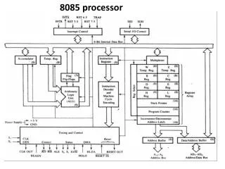
8085 Busses. Address Bus Data Bus Control Bus. The 8085 Architecture. Intel 8085 Pin Configuration. 3. Address & Data Bus. Address Bus The 8085 has eight signal lines, A15-A8, which are unidirectional and used as the high order address bus Multiplexed Address/Data Bus

8085 Busses
E N D
Presentation Transcript
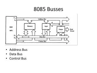
8085 Busses • Address Bus • Data Bus • Control Bus
Address & Data Bus • Address Bus • The 8085 has eight signal lines, A15-A8, which are unidirectional and used as the high order address bus • Multiplexed Address/Data Bus • The signal lines AD7-AD0 are bidirectional • They serve a dual purpose
Address & Data Bus • They are used as the low-order address bus as well as the data bus • In executing an instruction, during the earlier part of the cycle, these lines are used as the low-order address bus as well as the data bus • During the later part of the cycle, these lines are used as the data bus • However the low order address bus can be separated from these signals by using a latch
The Control and Status Signals There are 4 main control and status signals. These are: ALE: Address Latch Enable. This signal is a pulse that become 1 when the AD0 – AD7 lines have an address on them. It becomes 0 after that. This signal can be used to enable a latch to save the address bits from the AD lines. WR: Write. Active low. RD: Read. Active low. S1 and S0 : Status signals to specify the kind of operation being performed. Usually not used in small systems. IO/M: This signal specifies whether the operation is a memory operation (IO/M=0) or an I/O operation (IO/M=1).
Power supply and Clock Frequency • VCC- +5 V power supply • VSS – Ground reference • X0 and X1 • These are the inputs from the crystal or clock generating circuit. • The frequency is internally divided by 2.So, to run the microprocessor at 3 MHz, a clock running at 6 MHz should be connected to the X0 and X1 pins. • CLK (OUT): An output clock to use as system clock for other devices
Externally-Initiated Signals • Reset IN(Active low) • All operations are stopped and the program counter is reset to 0000. • Interrupt • The microprocessor’s operations are interrupted and the microprocessor executes what is called a “service routine”. • This routine “handles” the interrupt, (perform the necessary operations). Then the microprocessor returns to its previous operations and continues. • INTR,RST 5.5, RST 6.5, RST 7.5,TRAP
Externally-Initiated Signals • Ready • The 8085 has a pin called RDY. This pin is used by external devices to stop the 8085 until they catch up. • As long as the RDY pin is low, the 8085 will be in a wait state. • Hold • The 8085 has a pin called HOLD. This pin is used by external devices to gain control of the busses. • When the HOLD signal is activated by an external device, the 8085 stops executing instructions and stops using the busses. • This would allow external devices to control the information on the busses. Example DMA.
Communication between Microprocessor and Memory • To communicate with Memory, the MPU should be able to • Select the chip • Identify the register • Read from or write into register
Memory Map and Addresses • A memory map is a pictorial representation in which memory devices are located in the entire range of addresses. • Memory analogy with Notebook • Total Memory – Notebook • Chip - Page • Register - Line
A15 TO A0 00000000 00000000 | | 11111111 Chip select/ Register select Chip enable Memory address range 0000H to 00FFH
A15 TO A8 10000000 =80H Memory address range 8000H to 80FFH
Q Calculate the address lines required for 8 K-bytes(1024*8 =8192 registers) memory chip 13 • = 8192 13 Address lines
Data Bus Internal Data Bus Memory ALU Instruction Decoder B C D E H L SP PC 2000 2004 2005 4F 4F 2005 Control Logic MEMR Data Flow/ Instruction Fetch Operation