Understanding 8085 Microcomputer Architecture
Explore the basic architecture of the 8085 microcomputer, including major components like processor, control unit, memory, clock, and bus configuration. Learn about the architecture types, PIN configuration, registers, flags, timing, and control.

Understanding 8085 Microcomputer Architecture
E N D
Presentation Transcript
Microcomputer Major components of the computer - the processor, the control unit, one or more memory ICs, one or more I/O ICs, and the clock A single printed circuit board usually connects the ICs, making a computer called a microcomputer
Basic Architecture • Princeton and Harvard • Princeton Architecture* • Known as Von Neumann architecture • Single memory contains both the program code and the data. • Harvard Architecture • Two separate memories. One contains only data while the other is containing only program code.
Basic Architecture Princeton Harvard
Major components Processor Control Unit Memory Clock
Contents • Microprocessor Architecture
Microprocessor ? A microprocessor is multi programmable clock driven register based semiconductor device that is used to fetch , process and execute a data within fraction of seconds.
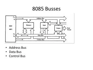
THE 8085 AND ITS BUSSES • The 8085 is an 8-bit general purpose microprocessor that can address 64K Byte of memory. • It has 40 pins and uses +5V for power. It can run at a maximum frequency of 3 MHz. • -The pins on the chip can be grouped into 6 groups: • Address Bus. • Data Bus. • Control and Status Signals. • Power supply and frequency. • Externally Initiated Signals. • Serial I/O ports.
The Address and Data Busses • The address bus has 8 signal lines A8 – A15 which are unidirectional. • The other 8 address bits are multiplexed (time shared) with the 8 data bits. • So, the bits AD0 – AD7 are bi-directional and serve as A0 – A7 and D0 – D7 at the same time. • During the execution of the instruction, these lines carry the address bits during the early part, then during the late parts of the execution, they carry the 8 data bits. • In order to separate the address from the data, we can use a latch to save the value before the function of the bits changes.
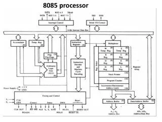
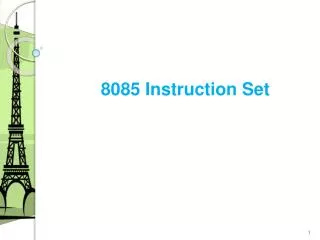
8085 ARCHITECTURE INTR INTA RST 5.5 RST 7.5 RST 6.5 SOD TRAP SID Interrupt controller Serial I/O controller 8 bit internal Data Bus Multiplexer Instruction Reg Temp Reg Accumulator Z temp W temp Reg array B C Flag Flip Flops D E Instruction Decoder and Machine Cycle Encoding H L Stack Pointer (16) ALU Program counter (16) Inc/dec latch Timing and control X1 Clk gen Data/ Address Buffer Address Buffer X2 Control Status DMA Reset S0 RD WR S1 ALE Clk out A15 –A8 Address Buss IO/M Reset out AD0 –AD7 Address/Data Buss HLDA HOLD Ready Reset in
Flag Register The flags are affected by the arithmetic and logical instruction D7 D6 D5 D4 D3 D2 D1 D0 S Z AC P CY
Accumulator • It is an 8 bit register • For any arithmetic and logical instruction one of the data should be in this register • It is used for storing the result of any arithmetic and logical manipulations. • It is also called as A register • All the data which are sent to I/O devices are sent via A register.
Temporary register • It is used to hold the data during the operation of arithmetic and logical operation
Sign Flag • If the D7 bit of the accumulator is set then this flag is set i.e 1 meaning that the result is in negative. • Ex. 7-8 = -1
Carry flag • During the arithmetic operation if a carry occurs then this flag is set. • Ex. F1+1F= 10 1 Carry
Zero flag • During the arithmetic/ logical operation if the result is zero then this flag is set. • Ex. FF-FF = 00
Parity flag • After the of the arithmetic and logical operation if the result is even then this flag is set. • Ex. 0A-02 = 08
Auxiliary carry flag • During BCD arithmetic operation when a carry is generated by D3 bit and passed on to D4 bit then this flag is set. • Ex. 1F+11 = 0000 1111 + 0001 0001 = 0010 0000
Timing and control • It synchronizes all the operation with the clock and generates the communication between the microprocessor and peripherals
Instruction Register and decoder • The instruction is loaded in the instruction register • The decoder decodes them and establishes the operation that has to be performed
Register array • The W and Z register are temporary registers • Used to hold the 8 bit data during the execution and it is used internally . • It is not used by the programmer.
Arithmetic and Logical unit • It is an 8 bit register • It is used for performing addition, subtraction and logical operation. • AND, OR, NOT, XOR, CMP are some of the logical operation.
Program Counter • It is a 16 bit register • It is used to point out the address of the next instruction which is to be executed
Stack pointer • It is a 16 bit register • It points the starting address of the stack .
Register Array • B, C, D, E, H and L are general purpose register • All are 8 bit register • If the are combined as BC, DE and HL they can store 16 bit data