Summary of PXD Session
250 likes | 410 Vues
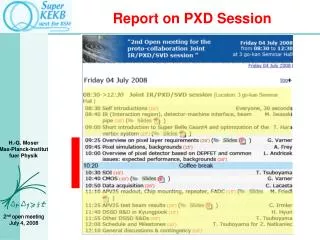
Summary of PXD Session. 1 Status of CAPS H. Hoedlmoser (Video) 2 Status of SOI Y. Arai 3 DEPFET Project C. Kiesling 4 Status of DEPFET R&D L. Andricek 5 DEPFET test beam P. Kodys. Vertexing at SuperBelle. Increased background Radiation damage Occupancy

Summary of PXD Session
E N D
Presentation Transcript
Summary of PXD Session 1 Status of CAPS H. Hoedlmoser (Video) 2 Status of SOI Y. Arai 3 DEPFET Project C. Kiesling 4 Status of DEPFET R&D L. Andricek 5 DEPFET test beam P. Kodys
Vertexing at SuperBelle • Increased background • Radiation damage • Occupancy Shorter readout times (SVD with APV25) Higher granularity: pixel detector 79mm => 75 mm: factor 1000 however: 10 ms integration time: factor 100 improvement Improve performance? Beam pipe: 0.66% X0 @ 1.5 cm: sip(MS) = 17 mm for 1 GeV/c (normal incidence) No need for very small pixels! 50 x75 mm2 ok It’s the material! => thin silicon! Keep beam pipe radius small ! Keep beam pipe thin!
CAPS H. Hoedlmoser, Hawaii Chattering pixels Problems due to SOI process Latch instead of flip-flop No chatter Back 11/2008
Binary readout CAP4 design Problem: ghost hits No ghosts for hexagonal readout Also for x-y readout
21x6 mm2 array 25 mm square pixels 100 MHz transfer in periphery 12 transferelines 72 outputs Occupancy: 5.2 x 10⁻⁵ @ 30 times current background (frame readout: ~ 10-2) Prototyp (CAP6) in production
SOI R&D Y. Arai
KEK SOIPIX History 2008.1 MPW run with KEK, LBNL, FNAL, Hawaii
Results Counting pixels (x-ray imaging) sBelle pixels: 48x48 pixels (100 x 100 mm2) Works, but problems due to back-gate-effect Successful with x-rays LBNL beam tests: best S/N (15) at U=10V Gets worse at higher U (no full depletion)
Plans Double the number of submissions at OKI Reduce back-gate-effect: Double SOI Implant through BOX 3D/SOI Project (with ZyCube) To be bonded in April 09 Second layer to shield substrate Reduce field under oxide 5-10 mm pitch
select Pixel matrix readout DEPFET Status • Each pixel is a p-channel FET on a completely depleted bulk • A deep n-implant creates a potential minimum for electrons under the gate • Signal electrons accumulate in the internal gate and modulate the transistor current (gq ~ 400 pA/e-) • Accumulated charge removed by a clear contact (“reset”) • Fully depleted: • large signal, fast signal collection • Low capacitance, • internal amplification: => low noise Frame readout => sequential readout of pixels or rows => rolling shutter mode => integration over many readout steps frame readout time: <10 ms => only few pixels active: low power => ASICs at periphery
7.6 cm @ R=1.3cm 9.6 cm @ R=1.8cm Detector Layout Small Detector: 20 – 24 Modules (one sensor each) Radii still subject to optimisation: Beam pipe radius: 1 cm or 1.5 cm? Probably: 1.5 cm initially with upgrade to 1.0 cm later Total detector: 6 Mpixel (2 layer) Most likely scenario Layer 1 at 1.8 cm Layer 2 at 2.2 cm Later upgrade: Layer 0 at 1.3 cm 2 or 3 layers Depends on machine design
z Z=0 Radius <-> Pitch Frame readout time < 10 ms Line readout time: 80 ns 2 x 4 lines per readout step -> 1000 lines along z Impact parameter resolution in z scales with R2 ! Extrapolation error ~ R Intrinsic resolution (pitch) ~ R Improvement: variable pitch At large z: larger pitch possible optimal charge sharing small cluster size Central part: small pitch better resolution
Z=0 SuperBelle PXD Module 50 x (75-115) mm2 (or variable in z) Read out four rows in parallel 256 x 1000 pixels 80 ns readout time 10 ms a frame (100 kHz) All silicon module 50 mm active area Thick frame X0 ~ 0.15% (average, including chips)
Test Beam Peter Kodys 2006 – 2008: 7 beam tests at DESY (<6 GeV) and CERN (180 GeV) Latest setup: 6 DEPFET array acting as telescope & DUT 20 M events taken => analysis in progress
Radiation Hardness The good news: DEPFET works after 8MRad with low noise The bad news: Large (operation mode dependent) threshold voltage shift & dispersion Annealing helps
Consequences (Idrain/A)1/2 gq Idrain 80-120 mA rough estimate: DUth -> 10% Dqg (min-max, rms should be smaller) Clear performance more critical! • Program: • ASICs deliver large voltage range • Operate (whenever possible) at 0V • Thinner oxides, optimal nitride/oxide • R&D program for optimized gate dielectric parallel to prototype production
Simulations Alexei Raspereza: Use LDC/LDC software Implement: Beam pipe DEPFET PXS SVD (no ghosts yet) CDC background PXD: 2 and 3 layer layout (Rinner=1.2cm and 1.7cm)
DEPFET performance DEPFET simulation verified/tuned to test beam data Cluster size in z at low q can be reduce by variable pitch Z-resolution at large q can be improved by variable pitch two options simulated 2 layer, Rinner=1.7cm 3 layer Rinner=1.2 cm Still not final!
Impact Parameter Resolution Adding Background: Resolution at low q degrades (however: software not yet tuned to low p) Occupancies: (initial lumi)
HEPHY IEKP Karlsruhe DEPFET Collaboration
Schedule Prototype Sensor Final Sensor ASICs Module Production Mechanics, Cooling Installation at KEK Ready: May 2013
Open Questions Radiation => improve on threshold voltage shift => dose, spectra, uniformity => optimal shielding => NIEL damage (particle type, spectra) Need to know beam pipe radius (outer!) => the smaller the better (for resolution)! => fix at latest mid 2010 (final sensor geometry) Need to know clearances and envelops at and around IP => mechanics, cooling, routing => temperature of the beam pipe Engineering of mechanics/interface to SVD => PXD should be mounted parallel to beam pipe => same mechanical structure as SVD? => common services (cooling)? DAQ interface (PXD may deliver up to 70 Gbit/s)
Conclusions CAPs, SOI: very promising concepts status: basic R&D important upgrade path for highest luminosity! DEPFET: evolving from basic R&D towards production Sensors: one more prototype production in 2009 (convert from ILC to SuperBelle layout) final production in 2011 radiation hardness should be improved Electronics: prototypes under test (control, readout) digital readout chip in work System: work started Schedule: install in 2013 upgrade after ~5 years (radiation damage, occupancy, smaller beam pipe?) We propose DEPFET as baseline PXD for superBelle to be discussed in closed session