SuperBelle Pixel Detector Overview: Requirements, Simulations, and Technologies
260 likes | 336 Vues
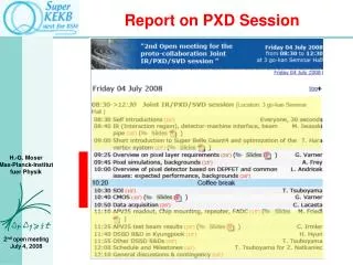
This report provides a comprehensive overview of pixel layer requirements, simulations, and technologies discussed at the PXD session by Varner, Frey, Andricek, Tsuboyama, and Lacasta. Topics include DEPFET, ASICs, SOI, CMOS, data rate, DAQ, and new technologies like 3D chips. Key conclusions highlight the need for robust vertexing, fast readout, and thin technologies for the SuperBelle pixel detector aiming for installation in 2013. The DEPFET technology stands out as the most realistic option based on initial assessments for long-term usability.

SuperBelle Pixel Detector Overview: Requirements, Simulations, and Technologies
E N D
Presentation Transcript
Pixel Simulations (A. Frey, Munich) Proposal: Consider Mokka framework (Geant4) for general superBelle MC
DEPFET Technology (A. Andricek, Munich) ASICs: DCD and Switcher are deep submicron technologies rad. hard beyond 10Mrad (with the appropriate design) DEPFETs: Not that easy … … noise performance seems to be okay up to 8 Mrad threshold shift could be compensated by re-adjustment of the Switcher voltages ∆Vt variation at higher TID (reason for this under investigation) and hence ∆ID at a given VGate has to be compensated by the DCD slightly higher noise of the f/e technological counter measures: thinner gate oxide reduces |∆Vt| further optimization of the gate dielectrics In conclusion: The DEPFET gets worse at high TIDs (8Mrad). Probably ok for several years of running
DEPFET Technology (A. Andricek, Munich) Thinning technology established 50 mm + frame All silicon ~0.14% X0 (average) Collaboration forming First superBelle prototypes 2010 (PXD5) Schedule to build complete detector till 2013
SOI Technology (T. Tsuboyama, KEK) 49 Mrad! Typical problem: Back gate effect Chip submitted, still waiting Similar project by Hawaii (same submission)
New Technologies: 3D Ron Lipton (Plenary)
New Technologies: 3D Ron Lipton (Plenary) • Test run with MIT: • VIP chip: 3 layer, no sensor • Low yield, many problems • Proof of principle! Continue with Tezzaron/Ziptonix • Powerful technology Time stamp DT = 300 ns: 1/33 reduction of Occupancy!
Conclusions Pixel Detector for SuperBelle should: allow robust vertexing at high background improve performance with respect to SVD2 => fast readout (or time stamp), thin Technologies: DEPFET SOI CMOS-MAPS 3D-technologie Aiming for installation in 2013 the DEPFET option seems to be the most realisitc (ok for running ~years at initial luminosity) => Tight schedule: start now! For final luminosity: consider ALL options