Download
1 / 58
1.71k likes | 4.42k Vues
BJT Transistor Modeling - I. Electronic Circuits First Term Second Year (11CS Batch). Model. A model is the combination of circuit elements, properly chosen, that best approximates the actual behaviour of a semiconductor device under specific operating conditions. Small Signal BJT Model.

E N D
BJT Transistor Modeling - I Electronic Circuits First Term Second Year (11CS Batch)
Model A model is the combination of circuit elements, properly chosen, that best approximates the actual behaviour of a semiconductor device under specific operating conditions. Small Signal BJT Model re Model Hybrid Parameter Model
Small Signal AC Analysis • Set all dc sources to zero and replace them by a short-circuit equivalent circuit. • Replace all capacitors by a short circuit equivalent. • Remove all elements bypassed by the short circuit equivalents introduced by steps 1 and 2. • Redraw the network in a more convenient and logical form.
AC Analysis Consider the following BJT circuit
AC Analysis Step 1,2,3: Step 4: Transistor Small Signal ac Equivalent Circuit
The Important Parameters: Zi, Z0, Av , Ai Input Impedance (Zi): Ii I0 Two-Port System + Zi + Z0 Vi V0 - -
Input Impedance (Cont.) RSense Two-Port System + Ii Zi Vi VS -
Example: For the system of the following Fig., determine the level of input impedance. RSense Two-Port System + 1k + Ii Zi VS 2mv Vi = 1.2 mv - - Solution:
Output Impedance (Z0) The output impedance is determined at the output terminals looking back into the System with the applied signal set to zero. The output impedance of a BJT amplifier is resistive in nature and, depending on the configuration and placement of the resistive elements, Z0 can vary from a few ohms to a level that can exceed 2 M.
Example: For the system of the following Figure, determine the level of output impedance. Solution:
Amplifier Gain • Gain • A multiplier that exists between the input and output of a circuit. • For example, if the gain of an amplifier is 100, then the output signal is 100 times as great as the input signal under normal operating conditions. • Types of Gain: • Voltage gain, AV • Current gain, Ai • Power gain, Ap
Voltage Gain The small signal ac voltage gain is defined as For the system of the above Fig., a load has not been connected to the output terminal, the gain is therefore referred to as no load voltage gain (AvNL). For the transistor amplifiers, the no load gain is greater than the loaded voltage gain.
AvNL + + Rs + Ii Zi VS V0 Using the Voltage Divider Rule Vi - - -
Rs BJT amplifier AvNL = 320 + + + 1.2k Example: For the BJT amplifier of the following Fig., determine Vi, Ii, Zi and Avs. Solution: Zi Vs = 40mv V0 = 7.68v Vi - - -
Current Gain (Ai) I0 BJT amplifier + + Vi Zi RL V0 - - From the circuit and
Example: For the given BJT circuit, determine: (a) Ii (b) Zi (c) V0 (d) I0 (e) Ai.
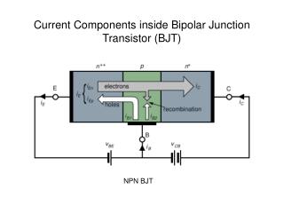
The re Transistor Model (a) Common Base (PNP) Configuration Ie Ie Ic re Ic =Ie
Ie Ic = Ie BJT Common-base Transistor amplifier I0 + + Vi Zi Z0 = RL V0 Voltage Gain: fV0 = -I0RL = -(-Ic)RL V0 = IeRL and Vi= IeZi = Iere Therefore, - - For the current gain
Example: For a common-base configuration with IE = 4mA, = 0.98, and an ac signal of 2mV applied between the base and ammeter terminals: • Determine the input impedance • Calculate the voltage gain if a load of 0.56 k is connected to the input terminals. • Find the output impedance and current gain. Solution: • Input Impedance = Zi = re = 2610-3/(410-3 ) = 6.5 (b) (c)
The re Transistor Model Ic Ic Common Emitter Configuration: Ic = Ib Ib Ib Ie (b) re Model (a) CE (NPN) Configuration
Ic = Ib Ii = Ib Ie vi vbe re Ii =Ib I0 = Ic = Ib BJT Common-emitter Transistor amplifier + + Vi Zi Z0 = RL V0 - -
Example: Given = 120 and IE = 3.2 mA for a common-emitter configuration with r0 = , determine: (a) Zi (b) Av if a load of 2 k is applied. (c) Ai with 2 k load. Solution: (a) (b) Av = -RL/re = -2000/8.125 = -246.15 (c) Ai = = 120
re Model for the Common-Emitter Configuration Note: r0 may be computed from the BJT output characteristics.
Common Emitter Fixed Biased Configuration (b) All capacitors and dc power supply removed (a) CE Fixed Bias Configuration (c) Circuit with the substitution of the re model
From Fig. (c) of the previous slide, the input impedance may be computed as Zi = RB ||reohms or In the majority of situations, RB10re. In such cases The output impedance is: Z0 = r0 ||RC or
If r0 10RC Voltage Gain: But or
But If r0 10RC, then or If r0 10RC and RB 10re , then Also, note that Current Gain:
Example: For the given network • Determine re. • Find Zi (with r0 = ). • Calculate Z0 (with r = ). • Determine Av (with r = ). • Find Ai(with r = ). • Repeat parts (c) through (e) including r = 50 k in all calculations and compare results. Solution: (a)
(b) (c) (d) (e) (f)
Input Impedance: Voltage Gain: But Output Impedance: If r0 10RC If r0 10RC
Current Gain: Where R’ = R1||R2 If r0 10RC Also note that
Example: For the network shown in the Fig., determine: • re (b) Zi (c) Z0 (r0 = ) (d) Av(r0 = ) (e) Ai (r0 = ) (f) The parameters of part (b) throughif r0 = 50 k. Solution: (a)
(b) (c) (d) (e) (f)
CE Emitter Bias Configuration Applying KVL to the input Side of Fig (b) we get Vi = Ibre + IeRE or Vi = Ibre + ( + 1)IbRE and the impedance Zb is: Fig. (a) or Fig. (b)
Since >> 1, therefore + 1 . • Zb re + RE • or Since RE is often much greater than re, the above equation is further reduced to Returning to Fig. (b), we have The output impedance Z0 is determined as:
CE Emitter Bias Configuration • Voltage Gain: and and for the approximation Zb RE Substituting Zb = (re + RE)
CE Emitter Bias Configuration Current Gain: Since In addition, I0 = Ib so that or
Example: For the network of the given Fig., determine (using appropriate approximations): (a) re (b) Zi (c) Z0 (d) Av and (e) Ai. Solution: • Testing RE > 10R2 (210)(0.68k) > 10(10k) 142.8k > 100k satisfied.
(b) The ac equivalent circuit is shown here. From this circuit The testing conditions r0 10(RC +RE ) and r0 10RC are both satisfied. Using the appropriate approximations yields Zb RE = 142.8 k Zi = RB||Zb = 9k||142.8k = 8.47k (c) Z0 = RC = 2.2k (d) Av = -RC/RE = -3.24 (e) Ai = -AvZi/RL = 144.1
Emitter Follower Configuration Emitter Follower Configuration re Model for EF Configuration
Emitter Follower Configuration Input Impedance (Zi): Zi = RB||Zb With ZB = re + ( + 1)RE. or Zb (re + RE) and Zb RE.
Emitter Follower Configuration Output Impedance (Z0): and Substituting for Zb gives or
Emitter Follower Configuration but and so that Since RE >> re, so If we now construct the network defined By the above equation:
Emitter Follower Configuration Since RE >> re Voltage Gain (AV): From the circuit given below We have
Emitter Follower Configuration From the Fig. or and or so that
Emitter Follower Circuit and since ( + 1) , or
Example: For the emitter follower network of the Fig., determine (a) re (b) Zi (c) Z0 (d) AV (e) Ai. Solution: (a) Zb = re + ( + 1)R = 334.56 k Zi = RB||ZB = 132.72k
(c) Z0 = RE||re = 12.56 (d) (e)