Download
1 / 11
110 likes | 240 Vues
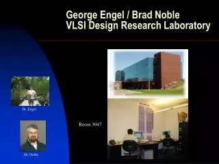
George Engel / Brad Noble VLSI Design Research Laboratory. Dr. Engel. Room 3047. Dr. Noble. Analog and Digital Electronics. Everest Biomedical Instruments. Building relationships!.

E N D
George Engel / Brad Noble VLSI Design Research Laboratory Dr. Engel Room 3047 Dr. Noble
Analog and Digital Electronics Everest Biomedical Instruments Building relationships!
The lab is well equipped with two SUN workstations, two HP workstations, a personal computer, several million dollars worth of CAD software, a large HP plotter, and a wide variety of test equipment including a modest setup for probing microchips. VLSI Design Research Laboratory Room 3047
FPGA Development $250,000 donation from Xilinx
Integrated Circuit (IC) Design Credit card reader IC for Magtek
BECS Technolgy, Inc. IC prototype for a local company! We did it all! Dr. Brad Noble Dr. George Engel Pranay Koka
HINP32C (Heavy-Ion Nuclear Physics, 32 Channel) is a 32 channel integrated circuit (IC) for use in a series of experiments in low- and intermediate-energy nuclear physics. The IC is fabricated in the AMIS 0.5 mm, N-well, double-poly, triple-metal, high-resistance C5N process through MOSIS. The die is 6 mm x 6 mm. VLSI Design Research Laboratory Room 3047
Questions????? VLSI Design Research Laboratory Room 3047