Download

1 / 38
410 likes | 1.25k Vues
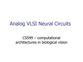
ADVANCED ANALOG VLSI DESIGN CENTER. ADVANCED ANALOG VLSI DESIGN CENTER. VLSI DESIGN CYCLE. VLSI DESIGN GUIDELINES. The L-Edit screen. Design Rule Checker. Menu Bar. Drawing Tools. Locator. Layer Palette. Work Area. Origin Marker.

E N D
The L-Edit screen Design Rule Checker Menu Bar Drawing Tools Locator Layer Palette Work Area Origin Marker
1.2 MICRON DOUBLE POLY, DOUBLE METAL ISO-CMOS DESIGN RULES 2.1.2 2.1.1 2.2 ploy 9.2 11.1 11.3 11.2 M1 9.3 9.1 2.5 2.3 M1 M1 PA PA M2 NA NA 2.4 2.6 M2
1.2 MICRON DOUBLE POLY, DOUBLE METAL ISO-CMOS DESIGN RULE 8.2.1 8.1 8.1.1 8.2.2 8.3.1 A V V 10.1 10.1 8.3.4 8.3.2 10.5 10.2 10.3 V V V M1 V 10.4 10.8 10.9.2 10.9.1 V V V V 10.7 10.6 10.6
1.2 MICRON DOUBLE POLY, DOUBLE METAL ISO-CMOS DESIGN RULE 1.1 1.2 PA 1.3 A 6.1 7.1
Three State Buffers Non-inverting buffer's timing waveform 100 D E F "Z" "Z"
Three State Buffer- The Third State Logic States: "0", "1" Don't Care/Don't Know State: "X" (must be some value in real circuit!) Third State: "Z" — high impedance — infinite resistance, no connection Tri-state gates: output values are "0", "1", and "Z" additional input: output enable (E) When E is high, this gate is a non-inverting "buffer" When E is low, it is as though the gate was disconnected from the output! This allows more than one gate to be connected to the same output wire, as long as only one has its output enabled at the same time
SUPER BUFFER Con’t ·(LN() - 1) = Cd / Cg =x
Selector Demultiplexer Selector: Choose I0 if S = 0 Choose I1 if S = 1 Demultiplexer: I to Z0 if S = 0 I to Z1 if S = 1
Well-formed Switching Networks Problem with the Demux implementation: multiple outputs, but only one connected to the input! The fix: additional logic to drive every output to a known value Never allow outputs to "float"
D-type flip-flop Q Q Bar