TEM Sample Preparation for Inorganic Materials
500 likes | 1.29k Vues
TEM Sample Preparation for Inorganic Materials • From transmission electron microscopy, people need thin (<100nm) samples • How are we going to make TEM samples that thin from bulk materials like a brick or an airplane? • Several methods - depends on initial form of

TEM Sample Preparation for Inorganic Materials
E N D
Presentation Transcript
TEM Sample Preparation for Inorganic Materials • From transmission electron microscopy, people need thin (<100nm) samples • How are we going to make TEM samples that thin from bulk materials like a brick or an airplane? • Several methods - depends on initial form of materials and what information is needed
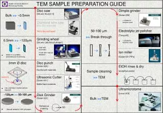
Sample Preparation – Hard Materials Samples • Powders (particles, fibers) • Bulk (stones, crashed planes) • Semiconductors (computer chips, devices) • How to prepare each of these?
Sample Preparation – Powders • If particle size is small enough to be electron transparent on its own (<100nm): – Add small amount of powder in solvent – Ultrasonicate to disperse particles well – Place a small drop of suspension on carbon-coated grids – Different types of carbon: amorphous, holey, lacey (increasing pores) • If particle size is larger: – Disperse particles in resin– Microtome using glass or diamond knives (depends on hardness of particles)?
Sample Preparation – Bulks • Some specimens can be prepared by just using mortar and pestle to crush the specimen into tiny pieces and then suspend the small particles in a nonaqueous solvent, and then catch the particles on a carbon film TEM grid. • Some specimens can be prepared by cutting the sample into thin slices using a diamond saw, then cutting 3-mm-diameter disks from the slice, thinning the disk on a grinding wheel, dimpling the thinned disk, then ion milling it to electron transparency.
Disk Cutting • Starting materials is ground or sliced (cleaved) to slabs about 500 um in thickness • Then the disc can be cut using ultrasonic disc cutter or the disc punch Ultrasonic Disc Cutter The Ultrasonic Disc Cutter is ideal for cutting TEM disks from brittle materials such as ceramics and semiconductors. Disc Punch The Disc Punch is ideal for cutting TEM disks from Metals
Mechanical Pre-thinning • Disc Grinder: produces high quality parallel-sided thin samples while reducing the chance of sample damage – Grind with SiC sandpaper (60 - 100 - 240 - 400 - 600 grit sizes) – Polish with Al2O3 or diamond suspensions (30 - 15 - 5 - 1 - 0.1μm)
TEM specimen preparation using the Tripod polishes • Wedge polishing – Mount sample to device with micrometer legs or variable angle head – Polish sample into a wedge shape - possible to produce electron transparent samples (thickness <0.5microns) – start with coarse grinds, then move to finer grits – Typically use diamond-impregnated plastic films rather than sand paper and diamond slurry – Used frequently for cross-sectional samples
Tripod polishes The point of interest is aligned with the back feet of the Tripod, to ensure the point of interest is coplanar with the back feet. Once the point of the interest has been reached, the polishing plane should be parallel with the back feet.
Tripod polishes General polishing sequence a. 30 um diamond film b. 15 um diamond film c. 3 um diamond film d. 1 um diamond film e. 0.5 um diamond film f. 0.05 um silica Process: Once the area of interest is located, the sample is polished using the tripod to generate an edged sample, with thickness of electron transparency.
Dimple Grinder • Advantages: • Large thin area with thicker rims; • Easier to handle fragile samples; • shorter preparation times; • easier location of the region of interest to be thinned; • large thin area in the center surrounded by thick rim eases handling of the thin samples.
How to use the Dimple Grinder • Generally, we use metallic wheel and 3 um diamond paste for dimple grinding stage, followed by: a. coarse polishing: using a ‘felt’ wheel and 3 um diamond paste. b. fine polishing: using a ‘felt’ wheel and 0.05 um alumina suspension. • We use boron nitride (BN) paste for dimpling metals and alloys. • Changes in color of transmitted light through a semiconductor (sometimes ceramics) can be used as a thickness indicator.
How to determine the thickness of Si(110) crystal by transparency colors?
Ion Milling – Bombard thin sample with energetic Ar ions, sputter away material until transparent – Ar is introduced into an electric field, ionized, accelerated at the sample as a plasma – Variables - ion current, angle of incidence, sample temperature, sample rotation, • High ion current – more damage • Smaller angle of incidence - less implantation, less damage, less preferential sputtering
Considerations for the Ion Milling Sputtering rate and artifact formation are two major factors in the process of ion milling of TEM specimens: What is sputtering: sputtering is the removal of atoms (atoms are knocked off) from the surface of a target by incident particles. Sputtering rate depends on: 1). Flux and velocity of the incident particles 2). Angle of incidence 3). Relative masses of the specimen atoms 4). Cohesive energy of the specimen atoms 5). Chemical interactions between incident particles and the specimen.
Available Techniques and Instrumentation There are three types of instruments available, including: 1). Conventional broad ion beam system 2). New generation ion beam system 3). Focused Ion Beam (FIB) system
Low Angle Ion Milling (down to 1 degree) Advantages of low angle milling using the single post: 1). Improved surface finish (ion polishing) 2). Larger thin areas while reducing artifacts 3). Less contamination from specimen surroundings 4). Reduced artifacts: (less amorphous layer, less contamination). Milling rates in the PIPS: Below list some typical milling rates at 4º obtained in the PIPS for various materials using one ion gun at 5 keV and no specimen rotation (um/hour for each gun) 1) Copper: 18 2) Silicon: 15 3) Silicon carbide: 8 4) Stainless steel 7 Precision Polishing Ion System (PIPS)
Specimen Preparation by Focused Ion Beam (FIB) Milling There are two different approaches to TEM sample preparation with FIB: lift out and traditional. Preference between the two depends on specific analytical conditions such as sample compositions. The life-out technique uses the milling action of the ion beam to excavate materials from both sides of the final thin section, and then cut the section free from the bulk specimen. An automated process lifting-out the delicate specimen and transferring it to a TEM specimen grid, is available in some FIB system. The traditional approach requires the use of manual cleaving and polishing techniques to create a pre-FIB sample that is small enough to fit into the TEM specimen chamber and thin enough (less than 50 mm) to minimize the amount of material that must be removed by the FIB. This pre-FIB specimen is then glued to TEM specimen grid and milled in the FIB to its final electron-transparent thickness.
FIB Instrument This is a dual beam system: SEM + FIB. Metal ions are accelerated into solid sample. Optically it is similar to a SEM. The system consist of: 1). Gun 2). Condenser lens (positive; electrostatic lenses, not magnetic lens as for electron). 3). Beam defining aperture (change spot size and beam current). 4). Beam blanker: faraday cage which brings beam out of optic axis and into bulk materials 5). Objective lens: change focal length 6). Scan coils 7). Stigmators FEI Nova 200 Nanolab
FIB ions source --- Liquid Metal Ion System (LMIS) 1). heat Ga metal above melting temperature; Ga flows to a W tip with radius ~2-5 um; Others sources: Au, Be, Si, Pd, Ni … 2). use field emission to form 2-5nm Ga tip (“Taylor cone”); 3). extract Ga+ ions and accelerate them down the column 4). Ga flow continuously replenishes source. The principal is a strong electromagnetic field causes the emission of positively charged ions. Why do we need ions instead of electrons: ions are bigger than electrons; they have high interaction Probability; since they have high mass, they have slow speed but high momentum and this is good for milling!
Ex-situ lift-out technique Extraction of the liberated lamella by electrostatic glass-needle under an optical microscope Transfer on TEM grid with carbon grid
In-situ lift-out technique a 200 nm lamella Extraction of the 200 nm lamella using a microgripper inside FIB (Kleindiek nanotechnik) Then transfer on TEM grid with carbon grid
Artifact Formation in the sample preparation • Surface topography: different thinning rates of components of the specimen; surface finish and cleanliness; crystallographic orientation; and milling angle • Structural artifacts include: amorphous surface layer; composition disproportionation; crystallographic imperfections like dislocation loop; structural changes due to excessive specimen heating.
Artifact Formation in the sample preparation Ion beam damage (see images at right): dislocations loop, point defects, amorphous particles deposition, non-uniform thickness, overheating, et al.