Chapter 2 Small-Signal Amplifiers
Chapter 2 Small-Signal Amplifiers. Most amplifiers in communication circuits are small signal amplifiers. Hence, they can be described by linear equations. We will consider several amplifiers including BJT, FET, operational amplifiers and differential amplifiers. Bipolar Transistor Amplifiers.

Chapter 2 Small-Signal Amplifiers
E N D
Presentation Transcript
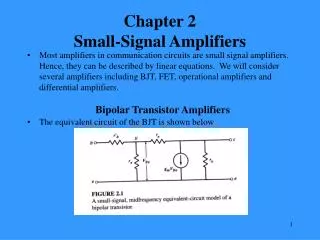
Chapter 2Small-Signal Amplifiers • Most amplifiers in communication circuits are small signal amplifiers. Hence, they can be described by linear equations. We will consider several amplifiers including BJT, FET, operational amplifiers and differential amplifiers. Bipolar Transistor Amplifiers • The equivalent circuit of the BJT is shown below
rb’ is the resistance between the terminal and the actual base junction, r is the base-emitter junction resistance. • Typically r >> rb’. An estimation of r is • r0 is the collector to emitter resistance typically of the order 15k, r is the collector-base resistance of the order several M. • The transconductance gm r = • A simplified version of the small-signal model equivalent circuit is given below
Common-Emitter Amplifier • here the coupling capacitance is treated as a short circuit. • The output voltage is therefore • The input impedance, not including Rs, is given be • Since r depends on applied the input resistance will depend on it as well. • The current gain is
The Circuit diagram and its equivalent circuit model for the CB amplifier are shown below • Since the sum of the currents leaving the emitter junction is 0, we have the following expression Common Base Amplifier
If r0 is assumed to be large compared with Rs, r and RL, the voltage gain is • if r >> Rs(1+), the magnitude of the voltage gain will be the same as that of the common-emitter amplifier • The input impedance of the common-base amplifier is determined using the following circuit
The output impedance is determined using the following circuit • The common-base amplifier has a voltage gain but its current gain is less than unity. It is used as non-inverting amplifiers where low input impedance and high output impedance is desired. • It also has much better high-frequency response than CE amplifier and is often used in high-frequency circuits.
Emitter Follower • The EF has a non-inverting voltage gain of less than 1 • However, it can combine with other stages, such as the CE stage, to realize a greater combined gain than CE stage alone
Using the equivalent circuit the voltage gain if found to be • EF configuration has the largest input impedance compared to the other configurations
The output impedance is • EF is used when low output impedance is needed. Also, although it has a voltage gain < 1, it has large current gain. It is frequently used as a power amplifier for low-impedance loads.
Field-Effect Transistors Amplifiers • There are two types of FETs -- JFETs and MOSFETs. • The low-frequency small signal model is as shown • The transconductance is defined as • For JFETs • where gm0 is the transconductance when gate-to-source bias voltage is 0, ID is the drain current and IDSS is the drain current when the gate-to-source voltage is 0. • For MOSFETs, gm is • where gmR is the transconductance at some specified drain bias current IDR
Common-Source Amplifier • The common-source amplifier is similar to the common-emitter amplifier • The common-source amplifier is similar to the common-emitter amplifier. • Normally Rg >> R so Vi = Vg
The source voltage is determined from the following equations • since the current leaving output node and source is zero • The current through Rs The source voltage is • The voltage gain is • If rd >> Rs and RL we have the following relationship • For gm Rs >> 1 we have
Source-Follower • The circuit diagram and its equivalent circuit model for source follower are shown below • If Rb >> Rs, then
Common-Gate Amplifier • The output impedance is • which is much smaller than the other two FET amplifier configurations and is the major advantage for this configuration • The common-gate amplifier is often used in high-frequency application and has a much larger bandwidth than the common source configuration.
Thus • The input impedance at the source can be found by solving for the source current • and • since
MultistageAmplifiers • The output impedance is determined as • but I0 is also the current passing through the source resistance so • The common gate amplifier has the highest output impedance of the three FET amplifier • Multistage amplifiers are used for impedance matching or to obtain extra gain. • Power transistors have smaller gain-bandwidth product than low-power transistors, hence the power amplification stage is often operated near unity voltage gain in order to maximize the bandwidth • Voltage amplification is carried out in the stages preceding the power amplification stage
Dual Gate FET • The FET cascode circuit has many high-frequency applications that two FETs are often fabricated as a single transistor with 2 gates. The source of the one transistor is continuous with the drain of the other so the device has 1 source, 1 drain and 2 gates • The device offers low-noise and high gain in radio-frequency applications • It is a versatile device which can be used as a mixer or automatic gain control amplifier. The equivalent circuit is as shown
Here gate 2 and the source are grounded • The load resistance of the first stage is the input resistance of the second stage, and the second stage is a common-gate amplifier. Therefore • Since • where gmR is the transconductance at some specified drain bias current IDR. • Since both transistors have the same drain current gm1=gm2. Thus Vi=-VD1 and Vgs2=-Vs2=-VD1
Push Pull Amplifiers • Transistors all exhibit a nonlinear characteristic that causes distortion of the input signal levels. Such distortion can be eliminated by push-pull amplifier • The above example uses 2 center-tapped transformers. The input transformer separates the input signal into 2 signal 180 out of phase. The output transformer is used to sum the output currents of the two transistors. • Hence • If the input signal is
then the output of the 2 transistors are also periodic, and they can be expressed in a Fourier series • If the two transistors are identical then I1 and I2 are identical except I2 lags I1 by 180 . Thus • The output current is • The even harmonics are eliminated from the output. This is important as FET have a square-law characteristic that generates a relatively large second harmonic.
Differential Amplifier • The differential amplifier is an essential building block in modern IC amplifiers. The circuit is shown below: • The operation of this circuit is based on the ability to fabricate matched components on the same chip. In the figure IEE is realized using a current mirror. We assume that Q1 and Q2 are identical transistors and both collector resistors fabricated with equal values. • The KVL expression for the loop containing the two emitter-base junctions is
The transistors are biased in the forward-active mode, the reverse saturation current of the collector-base junction is negligible. The collector currents IC1 and IC2 are given by • where we assumed that • where Vd is the difference between the two input voltages. KCL at the emitter node requires • Similarly The transfer • characteristic for the emitter-coupled pair is shown on the following page. • If Vd = 0 then IC1 = IC2
If we incrementally increase V1 by and simultaneously decrease V2 by . The differential voltage becomes . For < 4kT as indicated in the transfer characteristics above the circuit behaves linearly. IC1 increases by and IC2 decreases by the same amount.
Common Mode • Consider both V1 and V2 are increased by . The difference voltage remains 0, and IC1 and Ic2 remain equal. However, both IC1 and Ic2 exhibit a small increase . Hence the current in RE increases by . The voltage VE is no longer constant but increase by an amount of . This situation where equal signal are applied to Q1 and Q2 is the called the common mode. • Usually differential amplifiers are designed such that only differential signals are amplified. Analysis of Differential Amplifiers • The analysis of differential amplifiers is simplified using “half-circuit” concept. The equivalent circuit model for differential and common modes are shown:
Differential mode gain • Common mode gain is • The Common Mode Rejection Ration (CMRR) is defined as • From the above we obtain • If arbitrary signals V1 and V2 are applied to the inputs then
FET Differential Amplifier • A typical differential amplifier connection is shown below

