Download
1 / 31
330 likes | 654 Vues
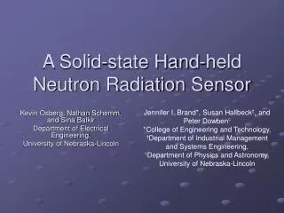
A Solid-state Hand-held Neutron Radiation Sensor. Jennifer I. Brand*, Susan Hallbeck † , and Peter Dowben ◊ *College of Engineering and Technology, † Department of Industrial Management and Systems Engineering, ◊ Department of Physics and Astronomy, University of Nebraska-Lincoln.

E N D
A Solid-state Hand-held Neutron Radiation Sensor Jennifer I. Brand*, Susan Hallbeck†, and Peter Dowben◊ *College of Engineering and Technology, †Department of Industrial Management and Systems Engineering, ◊Department of Physics and Astronomy, University of Nebraska-Lincoln Kevin Osberg, Nathan Schemm, and Sina Balkir Department of Electrical Engineering, University of Nebraska-Lincoln
Outline • Overview of the boron carbide diode for neutron detection • Hand-held neutron detector • Integrated front-end circuitry • Hand-held device • Experimental results • Ongoing work and conclusion
The Boron Carbide Diode as a Neutron Detection Sensor • Uses a specific isotope of boron, 10B, to detect neutrons
Detection efficiency for Various Neutron Sensitive Materials
Thin Neutron Detectors Semiconducting boron-carbide Conversion layer Neutron capture here yields no signal No electrical charges generated here by neutron capture Boron-10 + n Helium-4 Neutron capture that causes electrical charge generation Electrical charges generated by neutron capture products Lithium-7
Thick Neutron Detectors Semiconducting boron-carbide Conversion layer Neutron capture here yields no signal No electrical charges generated here by neutron capture Boron-10 + n Helium-4 Neutron capture that causes electrical charge generation Electrical charges generated by neutron capture products Lithium-7
History: Position paper on the device possibilities of a “theoretical” boron carbide semiconductor published jointly by the AEC and AFOSR 1958 Semiconducting Boron Deposition, by PECVD 1989 [J. Vac. Sci. Technol. A 7 (1989) 2796] Semiconducting Boron Carbide First Fabricated 1991 [Mat. Res. Soc. Symp. Proc. 190 (1991) 101–106] 1st BxCy U.S. Patent, Number 4,957,773 issued September 18th, 1990 Direct writing (single step CVD) of boron on a semiconductor substrate demonstrated 1991 [Applied Physics Lett.58 (1991) 607–609; chosen as a Synchrotron Radiation Center Highlight of 1992] First Boron Carbide/Silicon heterojunction diodes fabricated; 1992 boron carbide demonstrated to be an indirect adjustable band gap semiconductor material (0.7 eV < Eg < 1.9 eV) [Journ. Appl. Phys. 72 (1992) 4925–4933; Appl. Phys. A 58 (1994) 223–227] First boron carbide heterojunction fabricated by direct writing 1994 [Applied Phys. Lett.64 (1994) 1968–1970] 2nd BxCy US Patent, Number 5,468,978 issued Nov. 21, 1995
First boron carbide transistor fabricated 1996 • [Appl. Phys. Lett.68 (1996) 1495-1497] • First Boron Carbide Esaki tunnel diode • [J. Vac. Sci. Technol. B 14 (1996) 2957-2960] 1996 • First Boron Carbide Homojunction diode, stability of devices demonstrated to 220 °C • [Appl. Phys. Lett.70 (1997) 1028-1030] 1997 • 3rd BxCy US Patent, Number 5,658,834 issued Aug. 19, 1997 • 4th BxCy US Patent, Number 6,025,611, issued Feb. 15, 2000 • First Boron Carbide/silicon carbide heterojunction, stability of devices demonstrated to 350 °C • [Appl. Phys. Lett.79 (2001) 4357-4359] 2001 • First Boron Carbide neutron detector • [Appl. Phys. Lett.80 (2002) 3644-3646] 2001 • 5th BxCy US Patent, Number 6,440,786, issued August 27, 2002 • 6th BxCy US Patent, Number 6,600,177, issued July 29, 2003 • First Heteroisomeric Diode and all boron carbide neutron detectors • [J. Phys. Cond. Matter16 (2004) L139-L146; Mat. Sci. Eng. B 135 (2006) 129] 2004 • First Neutronvoltaic 2004 • 7th BxCy US Patent, Number 6,771,730, issued August 3, 2004 • 8th BxCy US Patent, Number 6,774,013, issued August 10, 2004 • First All Solid State Hand Held Neutron Detector Prototype 2006 • [IEEE Sensors Journal6 (2006) 1531-1538]
New Source Molecules for Boron Rich Semiconductors: J. Vac. Sci. Technol. A 10 (1992) 881 Icosahedron: most important strutural element of the boron-rich solids
The Boron Carbide Diode • Semiconducting boron carbide used to create a neutron sensitive diode • p and n type layers formed from molecules identical in formula but different in arrangement • Reverse bias applied to the diode sweeps charges out of depletion region, creating detectable current pulses through the diode
The Boron Carbide Diode • The diodes create a detectable, real-time response to a neutron capture • Resulting current pulses are in the range of hundreds of nanoamps for durations of 10 to 40 μsec, so the charge content is in the hundreds to thousands of fC
Charge Sensitive Amplifier • Charge sensitive amplifier converts current pulses to voltage pulses • Acts as a lossy integrator with RC feedback network, and gain of ~|1/Cf| • Cf realized by on-chip poly1/poly2 capacitors • Transistor MF controls the resistive feedback to change time constant
Charge Sensitive Amplifier Simulated diode pulses Charge amplifier output
Charge Sensitive Amplifier • In this application, the charge amplifier does suffer from non-linear gain • For large width and/or low charge content pulses, the resistive feedback interferes with the charge to voltage conversion • Example: A 3000fC charge transfer in 1μsec, and a 3000fC charge transfer in 10 μ sec
Charge Sensitive Amplifier • AMI 1.5 micron Standard CMOS Technology (1mm x 1mm die area) • Digitally selectable charge amplifier gain • Programmable bias voltages for tuning integrator time constant
Hand-Held Unit • The hand-held was designed around an Atmel microcontroller • Microcontroller samples charge amplifier output at 1.3 Msamples/sec with 12-bit resolution • Custom software modules allow for real-time processing of the waveform to determine resulting charge transfer per neutron
Hand-Held Unit • USB interface allows the hand-held to operate with computer for remote control and data capture • LCD display and rechargeable battery with a continuous operation time of 10 hours • Bias voltages for front-end can be controlled with 2mV of accuracy
Experimental Results • Operation of front-end tested with RC differentiator circuit to model boron carbide diode • 5pF feedback capacitor gives ideal gain of 200μV/fC • Measured gain based on RC circuit simulation gives a gain of ~170μV/fC
Experimental Results • Neutron testing was conducted with a paraffin moderated plutonium-beryllium source • Estimations of the source approximate the flux rate at 20 neutrons/msec over a 1cm2 area
Experimental Results • In this example, there are approximately 10 counts observed above a 1V threshold in 10msec • Based on the estimated flux rate, this gives a detection efficiency of 5% • If the threshold is reduced to 0.9V, the efficiency approaches 20%
Experimental Results • A typical measurement of particle detection applications is the pulse height spectra • Energy levels are quantized as channels, and each detected particle is assigned to a channel based on it’s energy • The number of events in each channel is then plotted versus the number of channels • The energy of the capture products is proportional to the amplitude of the resulting voltage pulse
Experimental Results • The blue curve is the pulse height spectra measured by the hand-held detector • The bottom curve is the predicted spectra based on the boron carbide diode detection characteristics • The red curve was measured when neutrons were blocked from the diode
Conclusions • Presented the complete design of a compact hand-held neutron detector • Experimental results verify the design approach and functionality • Real-time processing of the charge amplifier output agrees closely with predicted results
Ongoing Work • 0.5μm version of the integrated front-end designed using Cadence • Includes externally configurable filter to bandlimit output signal
Ongoing Work • Second generation hand-held detector using the 0.5 μm chip
Next Generation Application: Sensor Network Paradigm for Nuclear Proliferation Detection An Example 3-D Deployment of the Sensor Nodes as a Network: Cargo Container Inspection Processing Module Antenna Wireless Transmitter/ Receiver Sensing Module : Sensing diode Proposed Sensor Node • Objectives of Proposed Research: • The design, fabrication, and test of sensor node components: Sensing Module, Processing Module, Wireless Transmitter/Receiver • The design, fabrication, and test of a base station transmitter/receiver and the associated wireless sensor network protocol • Outcomes and Deliverables: • A neutron detection sensor network with low-power sensor nodes for nuclear proliferation detection • Physical dimensions of a single sensor node are similar to those of a business card for easy deployment • 3-D sensor node configurations that allow for neutron detection with directionality • Detection of fast neutrons (in addition to thermalized ones) by creating multiple wireless detection layers separated with moderators (such as paraffin) to slow down and capture certain fast neutrons (neutron spectroscopy application).