Download
1 / 23
230 likes | 359 Vues
Explore MOSFET structure, operation, electrostatics, gate voltage impact, and comparison with BJT. Learn about MOS capacitor as a parallel-plate capacitor in semiconductor devices. Gain insights into channel formation, voltage-dependent resistor, and device performance analysis.

E N D
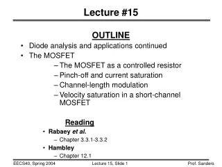
Lecture 15 OUTLINE • MOSFET structure & operation (qualitative) • Review of electrostatics • The (N)MOS capacitor • Electrostatics • Charge vs. voltage characteristic Reading: Chapter 6.1-6.2.1
GATE LENGTH, Lg OXIDE THICKNESS, Tox M. Bohr, Intel Developer Forum, September 2004 JUNCTION DEPTH, Xj CURRENT |GATE VOLTAGE| The MOSFET Metal-Oxide-Semiconductor Field-Effect Transistor: • Current flowing through the channel between the source and drain is controlled by the gate voltage. Gate Source Drain Substrate • “N-channel” & “P-channel” MOSFETs operate in a complementary manner • “CMOS” = Complementary MOS VTH
N-Channel MOSFET Structure Circuit symbol • The conventional gate material is heavily doped polycrystalline silicon (referred to as “polysilicon” or “poly-Si” or “poly”) • Note that the gate is usually doped the same type as the source/drain, i.e. the gate and the substrate are of opposite types. • The conventional gate insulator material is SiO2. • To minimize current flow between the substrate (or “body”) and the source/drain regions, the p-type substrate is grounded.
Review: Charge in a Semiconductor • Negative charges: • Conduction electrons (density = n) • Ionized acceptor atoms (density = NA) • Positive charges: • Holes (density = p) • Ionized donor atoms (density = ND) • The net charge density [C/cm3] in a semiconductor is • Note that p, n, ND, and NA each can vary with position. • The mobile carrier concentrations (n and p) in the channel of a MOSFET can be modulated by an electric field via VG.
Channel Formation (Qualitative) • As the gate voltage (VG) is increased, holes are repelled away from the substrate surface. • The surface is depleted of mobile carriers. The charge density within the depletion region is determined by the dopant ion density. • As VG increases above the threshold voltage VTH, a layer of conduction electrons forms at the substrate surface. • For VG > VTH, n > NA at the surface. The surface region is “inverted” to be n-type. VG < VTH VG ≥ VTH The electron inversion layer serves as a resistive path (channel) for current to flow between the heavily doped (i.e. highly conductive) source and drain regions.
Voltage-Dependent Resistor • In the ON state, the MOSFET channel can be viewed as a resistor. • Since the mobile charge density within the channel depends on the gate voltage, the channel resistance is voltage-dependent.
Channel Length & Width Dependence • Shorter channel length and wider channel width each yield lower channel resistance, hence larger drain current. • Increasing W also increases the gate capacitance, however, which limits circuit operating speed (frequency).
Comparison: BJT vs. MOSFET • In a BJT, current (IC) is limited by diffusion of carriers from the emitter to the collector. • IC increases exponentially with input voltage (VBE), because the carrier concentration gradient in the base is proportional to • In a MOSFET, current (ID) is limited by drift of carriers from the source to the drain. • ID increases ~linearly with input voltage (VG), because the carrier concentration in the channel is proportional to (VG-VTH) In order to understand how MOSFET design parameters affect MOSFET performance, we first need to understand how a MOS capacitor works...
MOS Capacitor • A metal-oxide-semiconductor structure can be considered as a parallel-plate capacitor, with the top plate being the positive plate, the gate insulator being the dielectric, and the p-type semiconductor substrate being the negative plate. • The negative charges in the semiconductor (for VG > 0) are comprised of conduction electrons and/or acceptor ions. In order to understand how the potential and charge distributions within the Si depend on VG, we need to be familiar with electrostatics...
Gauss’ Law r is the net charge density e is the dielectric permittivity If the magnitude of electric field changes, there must be charge! • In a charge-free region, the electric field must be constant. • Gauss’ Law equivalently says that if there is a net electric field leaving a region, there must be positive charge in that region: The integral of the electric field over a closed surface is proportional to the charge within the enclosed volume
Gauss’ Law in 1-D • Consider a pulse charge distribution: 0
Electrostatic Potential • The electric field (force) is related to the potential (energy): • Note that an electron (–q charge) drifts in the direction of increasing potential: 0
Boundary Conditions • Electrostatic potential must be a continuous function. Otherwise, the electric field (force) would be infinite. • Electric field does not have to be continuous, however. Consider an interface between two materials: Discontinuity in electric displacement eE charge density at interface!
MOS Capacitor Electrostatics • Gate electrode: • Since E(x) = 0 in a metallic material, V(x) is constant. • Gate-electrode/gate-insulator interface: • The gate charge is located at this interface. E(x) changes to a non-zero value inside the gate insulator. • Gate insulator: • Ideally, there are no charges within the gate insulator. • E(x) is constant, and V(x) is linear. • Gate-insulator/semiconductor interface: • Since the dielectric permittivity of SiO2 is lower than that of Si, E(x) is larger in the gate insulator than in the Si. • Semiconductor: • If r(x) is constant (non-zero), then V(x) is quadratic.
MOS Capacitor: VGB = 0 • If the gate and substrate materials are not the same (typically the case), there is a built-in potential (~1V across the gate insulator). • Positive charge is located at the gate interface, and negative charge in the Si. • The substrate surface region is depleted of holes, down to a depth Xdo Xdo 0 VS,o Qdep 0 -tox Xdo
Flatband Voltage, VFB • The built-in potential can be “cancelled out” by applying a gate voltage that is equal in magnitude (but of the opposite polarity) as the built-in potential. This gate voltage is called the flatband voltage because the resulting potential profile is flat. -tox 0 There is no net charge (i.e.r(x)=0) in the semiconductor under for VGB = VFB. 0 -tox
Voltage Drops across a MOS Capacitor • If we know the total charge within the semiconductor (Q̕S) , we can find the electric field within the gate insulator (Eox) and hence the voltage drop across the gate insulator (Vox): where QS is the areal charge density in the semiconductor [C/cm2] and is the areal gate capacitance [F/cm2] 0 -tox Xd
VGB < VFB (Accumulation) • If a gate voltage more negative than VFB is applied, then holes will accumulate at the gate-insulator/semiconductor interface. -tox 0 -tox Areal gate charge density [C/cm2]: 0
VFB < VGB < VTH (Depletion) • If the applied gate voltage is greater than VFB, then the semiconductor surface will be depleted of holes. • If the applied gate voltage is less than VTH, the concentration of conduction electrons at the surface is smaller than NA r(x) -qNA(x) Xd -tox 0 Areal depletion charge density [C/cm2]: 0 -tox Xd
VGB > VTH (Inversion) • If the applied gate voltage is greater than VTH, then n > NA at the semiconductor surface. • At VGB = VTH, the total potential dropped in the Si is 2fB where Xd,max -tox 0 -tox Xd,max
Maximum Depletion Depth, Xd,max • As VGB is increased above VTH, VS and hence the depth of the depletion region (Xd) increases very slowly. • This is because n increases exponentially with VS, whereas Xd increases with the square root of VS. Thus, most of the incremental negative charge in the semiconductor comes from additional conduction electrons rather than additional ionized acceptor atoms, when n exceeds NA. Xd can be reasonably approximated to reach a maximum value (Xd,max) for VGB ≥ VTH. • Qdep thus reaches a maximum of Qdep,max at VGB = VTH. • If we assume that only the inversion-layer charge increases with increasing VGB above VTH, then
Q-V Curve for MOS Capacitor inversion depletion accumulation