Download
1 / 11
110 likes | 227 Vues
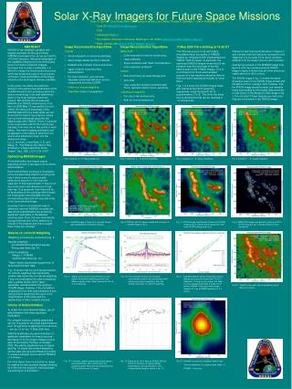
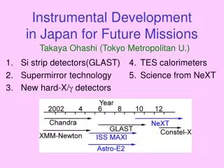
Instrumental Development in Japan for Future Missions. Takaya Ohashi (Tokyo Metropolitan U.). Si strip detectors(GLAST) Supermirror technology New hard-X/ g detectors. TES calorimeters Science from NeXT. Development of Silicon Strip Detector ( SSD ).

E N D
Instrumental Developmentin Japan for Future Missions Takaya Ohashi (Tokyo Metropolitan U.) • Si strip detectors(GLAST) • Supermirror technology • New hard-X/g detectors • TES calorimeters • Science from NeXT
Development of Silicon Strip Detector (SSD) Y. Fukazawa, T. Ohsugi et al. (Hiroshima U.) 0.01-1mm Position Reso. Good Time Reso.(a few ms) Stability/Radiation Hardness confirmed with accelerators. Small number of readout channels compared with pixel detectos Moderate Energy Resolution ~1keV(at 0℃) Thickness: 0.3-0.5mm Team in Hiroshima Univ. has developed SSDs for Astrophysics. For GLAST, GLAST-SSD(0.4mmt) SSD as Tracker of pair produced particles Single-Side Strip 0.23mm pitch, 384ch Achieved Large area (6 inch wafer) SSD technology will open a new era of GeV gammay-ray astronomy. 15cm
Mass Production is now running (10k SSDs for GLAST). Stable Performance and Low dead channels ( <0.01%) Depletion Voltage Leak Current 100V 200nA Double-Side SSD is now under development for Compton Gamma-ray Camera. Good scattering material with good position resolution Fast time resolution (for BGD rejection) Combination with CdTe is a good solution. (Candidate for NeXT) By Hiroshima U., SLAC, ISAS
Development of Hard X-ray Telescope ---Multilayer Supermirror --- K.Yamashita, Y.Tawara, H. Kunieda et al. (Nagoya U., ISAS) PSF : HPD = 2.1 arcmin • Balloon Experiment : InFOCuS, NUSMIT • Satellite Mission : NeXT, XEUS Focal length : 8 m Dia. 40 cm Energy band 20 - 40 keV FOV (fwhm) 9’ Ang. Resol. (HPD) 2’ Eff. Area 50 cm2 Replica foil mirrors and telescope [ InFOCuS-1 ]
NeXT • launch〜2010 • D= 60 cm, f=12 m • 6 modules • Seff= 1200 cm2@40 keV • HPD = 15 arcsec(goal) X-ray Reflectivity Pt/C ML Supermirror d=2.4-13 nm Reflectivity Energy (keV) NeXT Sensitivity 100 ks/5 s detection
CdTe 1cm VA2TA(IDE) ISAS Cadmium Telluride (CdTe) Diode Detector for Hard X-ray/Gamma-ray Observations T. Takahashi et al. (ISAS) • High Z semiconductor (ZCd = 48, ZTe = 52) • High density(5.8 g/cm3) • Room Temperature Operation (Eg ~ 1.5 eV) • High Resolution CdTe Diode by ISAS • Applications • Focal plane detector of the Hard X-ray Mirror • Next Generation Compton Telescope First Prototype (pixel size 625μmx625μm) 400 pixels
T.Takahashi et al (ISAS, SLAC, Hiroshima U., U. Tokyo. Osaka U.) New Gamma-ray Detector for the NeXT - Compton Kinematics - g Incident angle of g-rays is defined by an active collimater CdTe/Si Strip or Pixel Ein g E1 θ E2 Background events (activation / intrinsic, shield leakage) can be reduced significantly by requiring this relation for E1 and E2. ISAS
Development of High Resolution X-ray Spectrometer 1m K. Mitsuda et al. (ISAS, Tokyo Metr. U., ) Astro-E2 XRS (2005~) 32 pixel semiconductor- calorimeter array 2.5 mm×5.3 mm (1.9’ ×4.1’ ) ΔE ~ 10 – 12 eV 3 year life time of coolant NeXT Large format array of (~ 32x32 pixel) TES calorimeter (ΔE ~ 3 eV) TES (Transition Edge Sensor) Using sharp edge at normal to superconductor transition Higher sensitivity of thermometer Faster response by electro-thermal feedback (Irwin et al. 2000, NIMA 444, 184)
Present Performance of 1m 1.7 mm Si TES 0.5 mm 0.5 mm Yesterday! TES Calorimeter TES calorimeter fabricated by Seiko Instruments Inc. Tc=105 mK α≡ dlnR/dlnT ~ 100 9.2±0.4 eV Ka1 (5.899 keV) Mn - Ka2 (5.888 keV) 0.5 x 0.5 mm Ti / Au bilayer TES0.3 x 0.3 mm Au absorber, Ti/Au/Au=40/110/300 nm thick
Making of Large Format Array Experimental production of mushroom-shaped Sn absorber 16 x 16 calorimeter array structure 1 mm size 500mm Through hole wiring electrodeposit Sn & polish it to 8 μm thick
Chandra, XMM .... 1999 Astro-E2 .............. 2005 NeXT ................. ~2010 NeXT: Dynamics and Acceleration in the Universe