Advanced Wafer Level Packaging Technologies for Customized Applications
260 likes | 444 Vues
Learn about Wafer Level Packaging (WLP) and its electrical I/O schemes (TSV) from a foundry perspective. WLP options include low temperature metal alloy bond, glass frit bond, anodic bonding, silicon fusion bonding, and more. Explore the benefits, considerations, and applications of each bonding technology.

Advanced Wafer Level Packaging Technologies for Customized Applications
E N D
Presentation Transcript
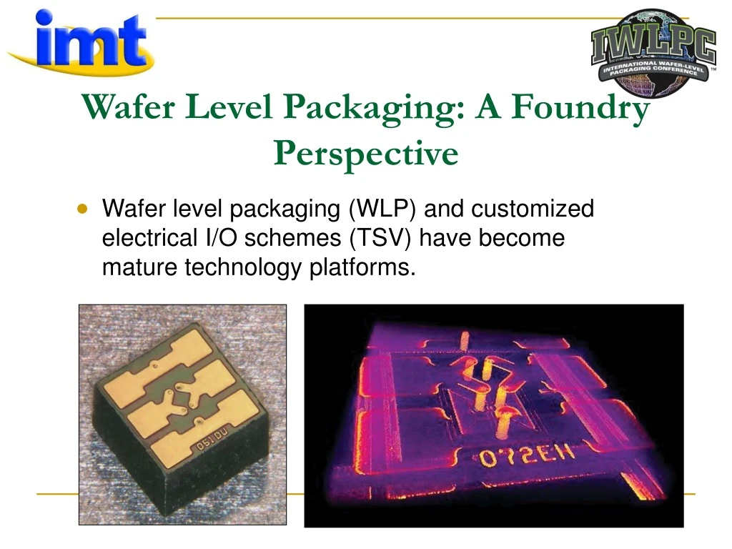
Wafer Level Packaging: A Foundry Perspective • Wafer level packaging (WLP) and customized electrical I/O schemes (TSV) have become mature technology platforms.
WLP is generally customized to meet specific customer requirements: • Die Size • Temperature Budget • Materials Used • Hermiticity Requirements • Absolute Pressure • Specialized Packaging
Wafer Level Packaging Options • Low Temperature Metal Alloy Bond • High Production Yields (99.1%) – based on 158.000 dies and 592 wafers • Low Temperature Bond (160 to 190 C) with High Reflow Temperature (> 500 C) • Narrow Bond Line Width (50 to 100 mm) • Tightly Controlled Bond Line Thickness (+/- 5 mm) • Topography Tolerant (Up to 7000 A) • High Bond Strength
Low Temperature Metal Alloy Bond (Continued) • Electrically Conductive • Hermetic • Compatible across multiple substrates • Hermiticity verified on a die by die basis by electrically probing in package thermistors
Low Temperature Metal Alloy Bond (Continued) • The reliability of this bond technology was verified a number of time by independent laboratories. • 96 hour autoclave at 2 ATM and 121 C • SF6 bombing for 1487 hours • Air bombing for 1295 hours at 2 ATM • Air bombing for 200 hours at 150 C • 85 C / 85% RH exposure for 1262 hours
Glass Frit Bond • Low cost • Hermetic • High vacuum (<1 mTorr) • Bond line widths ~ 400 mm • Bond Temperature (400 C) • Compatible with getter activation • Extremely Strong • Withstand 12,000 G acceleration loads
Glass Frit Bond (Continued) • Topography tolerant • Can go over active circuits • Providing the correct metallurgy is selected • Well characterized reliability Wafer Aligner Wafer Bonder
Anodic Bonding • Excellent technology for bonding silicon and glass wafers • Low temperature (300 C) and low voltage (300 V) is now mature • Hermetic • Not topography tolerant • Bond line widths ~200 mm • Bond strength similar to glass frit • Excellent reliability characteristics
Silicon Fusion Bonding • First demonstrated in 1986 and now very mature technology • Enables the production of complex structures by combining by combining two or more patterned and etched wafers • Bond is extremely strong and hermetic • Wafers must be atomically clean and smooth • Prior to bond a hydrophilization step is required but this is very predictable • Main drawback, high post bond annealing temperatures (~ 1000 C) • Prohibits any metals
Au / Au Thermo-Compression Bond • Hermetic • Sputter deposited bond line ~ 50 mm in width • Bond temperature ~ 300 C • Bond line loading > 5 MPa • Not topography tolerant • Bond strength not as high as glass frit but higher than eutectic • Some commercial bonding systems cannot generate enough clamp force
Polymer bonding • Not hermetic • Effective as a particulate contamination barrier and resistant to fluid penetration • Used widely in micro-fluidic circuits • Low cost • Lithographyically defined bond lines • Widths and heights can vary widely to suit various applications • Bond temperature low (~ 200 C)
WLP Summary • All six of the bond technologies reviewed are mature production worthy options • Tens of thousands of successful bonds have demonstrated the value of wafer level packaging • Sophisticated wafer bonding systems are manufactured by several companies • All of the discussed bonds can be performed on these systems • Critical component in 3D packaging • Allows integration of heterogeneous technologies • Reduces packaging cost • Allows package size reduction
WLP Summary (Continued) • When choosing a bond technology various factors need to be considered: • Die size and design • Available bond line real estate • Die topography • Device temperature budget • Vacuum and hermiticity requirements • Die packaging environment • Bond line electrical conductivity or dielectric property considerations
Electrical I/O Configurations, Through Silicon Vias (TSV) • Typical configuration, Solid Copper via with SiO2 insulation through one if the two wafers making up the bonded pair Lid Wafer and Device Cavity WLP Bond Line TSV Back Side Circuits And Bumps Note, the bond line can be patterned to be an electrical circuit
Electrical I/O Configurations, Through Silicon Vias (TSV) • Typical RF performance data for TSV • Single via adds only ~0.01 bB of loss of loss at 6 GHz
Electrical I/O Configurations, Through Silicon Vias (TSV) • Historically, the industry has struggled making TSV void free. • Recent process advances have overcome this problem • 150,000 TSV in a 150 mm wafer with a via yield of 99.9%
Electrical I/O Configurations, Through Silicon Vias (TSV) • There are specific via design rules that need to be followed 50 x 250um in Reliability testing 50 x 500um demonstrated
Electrical I/O Configurations, Through Silicon Vias (TSV) • There is virtually no change in via resistance as a function of temperature cycling
Electrical I/O Configurations, Through Silicon Vias (TSV) • Summary • Creation of metal filled vias is a mature high yielding process technology within the MEMS industry • TSV technology is the next logical step in providing vertical integration in the semiconductor market driven by space constraints in hand held mobile devices • TSV are a major component in 3D packaging
Electrical I/O Configurations, Through Silicon Vias (TSV) • Summary (Continued) • Metal filled vias have the following attributes: • Low resistance (0.01 Ohms per via) • Low insertion loss for RF applications • A vehicle to allow die shrinkage • Can vary in diameter from 15 to 50um • Can go completely through a 500um wafer • Are electrically isolated from the silicon • Are compatible with high volume, low cost post wafer chip processing • Can be fabricated with a high via yield (99.96%)
Conclusion WLP Plus TSV • The combination of these two technologies provide significant advantages to MEMS designers in the following areas: • Low pressure, low cost packaging • Low insertion loss electrical I/Os • Low resistance I/Os • Smaller chip sizes