Download
1 / 16
160 likes | 302 Vues
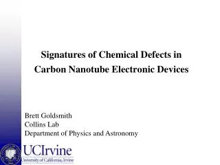
Signatures of Chemical Defects in Carbon Nanotube Electronic Devices. Brett Goldsmith Collins Lab Department of Physics and Astronomy. A broad look at defects. Tools to Study CNT Defects. Fan, Nature Materials. December, 2005. Drain. Source. V SD. V F. V tip.

E N D
Signatures of Chemical Defects in Carbon Nanotube Electronic Devices Brett Goldsmith Collins Lab Department of Physics and Astronomy
Tools to Study CNT Defects Fan, Nature Materials. December, 2005
Drain Source VSD VF Vtip Scanning Probe Microscopy - KFM • Kelvin Force Microscopy (KFM): • Records forces between tip and sample • Measures Surface Potential • Allows indirect measurement of local resistance Source Drain
Drain Source VSD VF Vtip Scanning Probe Microscopy - SGM • Scanned Gate Microscopy (SGM): • Records current through the nanotube circuit • Measures local field sensitivity • Shows where the device is “gate sensitive” topography topography + SGM
Growth Defects - KFM Ballistic Nanotube Nanotube with Growth Defects
Growth Defects – KFM detail Ballistic Nanotube Nanotube with Growth Defects:
Growth Defects - SGM topography topography + SGM
WE RE CE Vg Defect Creation on Nanotubes • Many ways to create defects: • Mechanical • Chemical • Irradiation • Electrochemical Jaan Mannik V18.7
Basic Effects of Oxidation Weak Oxidation
Basic Effects of Strong Oxidation Strong Oxidation
Mild Oxidation - SGM topography topography + SGM
One SWNT after Progressively Harsh Treatments • Surface Potential along as-grown CNT: Surface Potential after mild oxidation: Surface Potential after strong oxidation:
Weak Defects - KFM Mildly Oxidized Nanotube Ballistic Nanotube
Summary • Microscopy techniques such as KFM and SGM show that oxidation and growth defects have similar effects on CNT circuits. Dr. Yuwei Fan Dr. Jaan Mannik Brett Goldsmith Alex Kane Derek Kingrey Bucky Khalap Kevin Loutherback Fatima Alim Yasser Elliasal ACS-PRF