Multiple function unit design
Design a unit that can perform both addition and subtraction operations. Simplify the design by utilizing one's complement and selective addition technique. Explore alternate design methods for efficient computation.

Multiple function unit design
E N D
Presentation Transcript
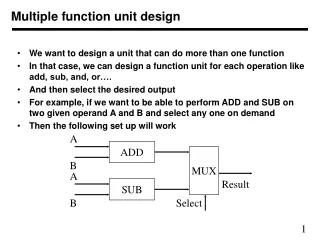
A A MUX ADD SUB B B Result Select Multiple function unit design • We want to design a unit that can do more than one function • In that case, we can design a function unit for each operation like add, sub, and, or…. • And then select the desired output • For example, if we want to be able to perform ADD and SUB on two given operand A and B and select any one on demand • Then the following set up will work
a a a b b b 1-bit sub 1-bit sub 1-bit sub w w w r r r Design of a SUB unit • An n-bit subtract unit can be designed in the same way as an n-bit adder • One bit subtract unit: It has two inputs a and b (b is subtracted from a) and a borrow (w) in case the previous stage had one • It produces an output (result) and a borrow (cascading output) • Borrow from one stage is fed from a stage to the next stage • Truth table is shown • An n-bit subtract circuit is shown
Simplifying ADD/SUB unit design • Separate ADD and SUB units are expensive • We can simplify the design • SUB is same as adding negation of B to A • How to negate? • Take one’s complement and add 1 • Adding one is also expensive • It needs an n-bit adder • However, we only need to add two bits in each stage • In the first stage we need to add 1’s complement of first bit and 1 • In other stages, we need to a carry output to 1’s complement of bit • We select B or negative of B depending on the requirement • We add A to the selected input to obtain the result
ADD/SUB ADD/SUB ADD/SUB 1 0 1 0 1 0 MUX MUX MUX b b b a a a 1-bit add 1-bit add 1-bit add c c c ADD/SUB s s s Alternate ADD/SUB unit design • 2’s complement generation of B is expensive • For subtract, we can take 1’s complement of B and add it to A • Then we need to add 1 to the result • This can be achieved by adding 1 as input carry to n-bit adder • For Add operation, we simply add B to A with carry = 0 • Signal ADD/SUB = 0 for Add and 1 for Sub • The block diagram is shown below • MUX and inverter can be replaced by XOR of b and ADD/SUB