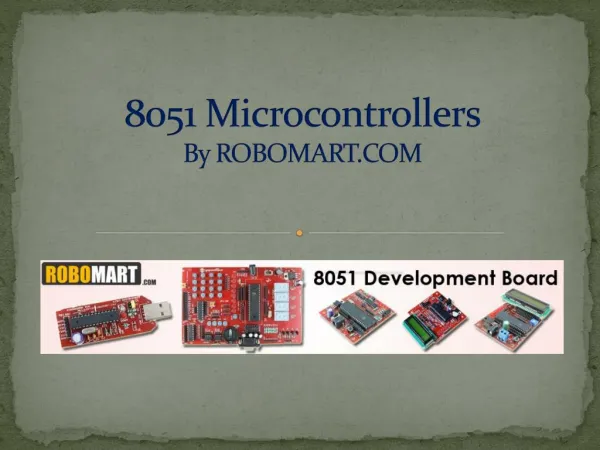
The 8051 Microcontroller
The 8051 Microcontroller is a versatile embedded system with 4KB internal ROM, 128 bytes of RAM, and four 8-bit I/O ports (P0-P3). It features two 16-bit timers/counters and one serial interface, making it suitable for numerous applications. Designed for efficiency, the 8051 supports external memory, is cost-effective, and offers a range of I/O options. Embedded systems like keyboards, printers, and automotive controls utilize microcontrollers like the 8051 for specific tasks. This guide explores its architecture, pin configuration, and essential functionalities for developers.


The 8051 Microcontroller
E N D
Presentation Transcript
8051 Basic Component • 4K bytes internal ROM • 128 bytes internal RAM • Four 8-bit I/Oports (P0 - P3). • Two 16-bit timers/counters • One serial interface CPU RAM ROM A single chip Serial COM Port I/O Port Microcontroller Timer
Block Diagram External Interrupts Interrupt Control 4k ROM 128 bytes RAM Timer 1 Timer 2 CPU OSC Bus Control 4 I/O Ports Serial RXD P0 P2 P1 P3 TXD Addr/Data
Other 8051 featurs • only 1On chip oscillator (external crystal) • 6 interrupt sources (2 external , 3 internal, Reset) • 64K external code (program) memory(only read)PSEN • 64K external data memory(can be read and write) by RD,WR • Code memory is selectable by EA (internal or external) • We may have External memory as data and code
Embedded System(8051 Application) • What is Embedded System? • An embedded system is closely integrated with the main system • It may not interact directly with the environment • For example – A microcomputer in a car ignition control • An embedded product uses a microprocessor or microcontroller to do one task only • There is only one application software that is typically burned into ROM
Examples of Embedded Systems • Keyboard • Printer • video game player • MP3 music players • Embedded memories to keep configuration information • Mobile phone units • Domestic (home) appliances • Data switches • Automotive controls
Three criteria in Choosing a Microcontroller • meeting the computing needs of the task efficiently and cost effectively • speed, the amount of ROM and RAM, the number of I/O ports and timers, size, packaging, power consumption • easy to upgrade • cost per unit • availability of software development tools • assemblers, debuggers, C compilers, emulator, simulator, technical support • wide availability and reliable sources of the microcontrollers
Comparison of the 8051 Family Members • ROM type • 8031 no ROM • 80xx mask ROM • 87xx EPROM • 89xx Flash EEPROM • 89xx • 8951 • 8952 • 8953 • 8955 • 898252 • 891051 • 892051 • Example (AT89C51,AT89LV51,AT89S51) • AT= ATMEL(Manufacture) • C = CMOS technology • LV= Low Power(3.0v)
Comparison of the 8051 Family Members WD: Watch Dog Timer AC: Analog Comparator ISP: In System Programable
EA/VPP ALE/PROG PSEN (INT0)P3.2 (INT1)P3.3 (WR)P3.6 (RD)P3.7 8051 Foot Print Vcc P1.0 1 40 P0.0(AD0) P1.1 2 39 P0.1(AD1) P1.2 3 38 P0.2(AD2) P1.3 4 37 8051 (8031) (8751) (8951) P0.3(AD3) P1.4 5 36 P0.4(AD4) P1.5 6 35 P0.5(AD5) P1.6 7 34 P0.6(AD6) P1.7 8 33 P0.7(AD7) RST 9 32 (RXD)P3.0 10 31 (TXD)P3.1 11 30 12 29 P2.7(A15) 13 28 (T0)P3.4 P2.6(A14) 14 27 (T1)P3.5 P2.5(A13) 15 26 P2.4(A12) 16 25 P2.3(A11) 17 24 P2.2(A10) XTAL2 18 23 P2.1(A9) XTAL1 19 22 P2.0(A8) GND 20 21
IMPORTANT PINS (IO Ports) • One of the most useful features of the 8051 is that it contains four I/O ports (P0 - P3) • Port 0 (pins 32-39):P0(P0.0~P0.7) • 8-bit R/W - General Purpose I/O • Or acts as a multiplexed low byte address and data bus for external memory design • Port 1 (pins 1-8):P1(P1.0~P1.7) • Only 8-bit R/W - General Purpose I/O • Port 2 (pins 21-28):P2(P2.0~P2.7) • 8-bit R/W - General Purpose I/O • Orhigh byte of the address bus for external memory design • Port 3 (pins 10-17):P3(P3.0~P3.7) • General Purpose I/O • if not using any of the internal peripherals (timers) or external interrupts. • Each port can be used as input or output (bi-direction)
Read latch Vcc TB2 Load(L1) P1.X pin Internal CPU bus DQ ClkQ P1.X M1 Write to latch TB1 Read pin Hardware Structure of I/O Pin
Hardware Structure of I/O Pin • Each pin of I/O ports • Internally connected to CPU bus • A D latch store the value of this pin • Write to latch=1:write data into the D latch • 2 Tri-state buffer: • TB1: controlled by “Read pin” • Read pin=1:really read the data present at the pin • TB2: controlled by “Read latch” • Read latch=1:read value from internal latch • A transistor M1 gate • Gate=0: open • Gate=1: close
Read latch Vcc Load(L1) P1.X pin Internal CPU bus DQ ClkQ P1.X M1 Write to latch Read pin Writing “1” to Output Pin P1.X TB2 2. output pin is Vcc 1. write a 1 to the pin 1 output 1 0 TB1
Read latch Vcc Load(L1) P1.X pin Internal CPU bus DQ ClkQ P1.X M1 Write to latch Read pin Writing “0” to Output Pin P1.X TB2 2. output pin is ground 1. write a 0 to the pin 0 output 0 1 TB1
Read latch Vcc Load(L1) P1.X pin Internal CPU bus DQ ClkQ P1.X M1 Write to latch Read pin Reading “High” at Input Pin 2. MOV A,P1 external pin=High TB2 • write a 1 to the pin MOV P1,#0FFH 1 1 0 TB1 3. Read pin=1 Read latch=0 Write to latch=1
Read latch Vcc Load(L1) P1.X pin Internal CPU bus DQ ClkQ P1.X M1 Write to latch Read pin Reading “Low” at Input Pin 2. MOV A,P1 external pin=Low TB2 • write a 1 to the pin • MOV P1,#0FFH 1 0 0 TB1 3. Read pin=1 Read latch=0 Write to latch=1 8051 IC
Vcc 10 K Port 0 P0.0 P0.1 DS5000 8751 8951 P0.2 P0.3 P0.4 P0.5 P0.6 P0.7 Port 0 with Pull-Up Resistors
IMPORTANT PINS • PSEN (out): Program Store Enable, the read signal for external program memory (active low). • ALE (out): Address Latch Enable, to latch address outputs at Port0 and Port2 • EA (in): External Access Enable, active low to access external program memory locations 0 to 4K • RXD,TXD: UART pins for serial I/O on Port 3 • XTAL1 & XTAL2: Crystal inputs for internal oscillator.
Pins of 8051 • Vcc(pin 40): • Vcc provides supply voltage to the chip. • The voltage source is +5V. • GND(pin 20):ground • XTAL1 and XTAL2(pins 19,18): • These 2 pins provide external clock. • Way 1:using a quartz crystal oscillator • Way 2:using a TTL oscillator • Example 4-1 shows the relationship between XTAL and the machine cycle.
C2 XTAL2 30pF C1 XTAL1 30pF GND XTAL Connection to 8051 • Using a quartz crystal oscillator • We can observe the frequency on the XTAL2 pin.
XTAL2 NC EXTERNAL OSCILLATOR SIGNAL XTAL1 GND XTAL Connection to an External Clock Source • Using a TTL oscillator • XTAL2 is unconnected.
Machine cycle • Find the machine cycle for • (a) XTAL = 11.0592 MHz • (b) XTAL = 16 MHz. • Solution: • (a) 11.0592 MHz / 12 = 921.6 kHz; • machine cycle = 1 / 921.6 kHz = 1.085 s • (b) 16 MHz / 12 = 1.333 MHz; • machine cycle = 1 / 1.333 MHz = 0.75 s
Pins of 8051 • RST(pin 9):reset • input pin and active high(normally low). • The high pulse must be high at least 2 machine cycles. • power-on reset. • Upon applying a high pulse to RST, the microcontroller will reset and all values in registers will be lost. • Reset values of some 8051 registers • power-on reset circuit
Vcc 31 EA/VPP X1 10 uF 30 pF X2 RST 9 8.2 K Power-On RESET
RESET Value of Some 8051 Registers: Register Reset Value PC 0000 ACC 0000 B 0000 PSW 0000 SP 0007 DPTR 0000 RAM are all zero
Pins of 8051 • /EA(pin 31):external access • There is no on-chip ROM in 8031 and 8032 . • The /EA pin is connected to GND to indicate the code is stored externally. • /PSEN & ALE are used for external ROM. • For 8051, /EA pin is connected to Vcc. • “/” means active low. • /PSEN(pin 29):program store enable • This is an output pin and is connected to the OE pin of the ROM. • See Chapter 14.
Pins of 8051 • ALE(pin 30):address latch enable • It is an output pin and is active high. • 8051 port 0 provides both address and data. • The ALE pin is used for de-multiplexing the address and data by connecting to the G pin of the 74LS373 latch.
Address Multiplexing for External Memory Figure 2-7 Multiplexing the address (low-byte) and data bus
Address Multiplexing for External Memory Figure 2-8 Accessing external code memory
Accessing External Data Memory Figure 2-11 Interface to 1K RAM
WR RD PSEN OE ALE 74LS373 CS G P0.0 P0.7 A0 A7 D D0 D7 EA P2.0 P2.7 A8 A15 8051 External code memory ROM
WR WR RD RD PSEN ALE 74LS373 CS G P0.0 P0.7 A0 A7 D D0 D7 EA P2.0 P2.7 A8 A15 RAM External data memory 8051
WR WR RD RD PSEN ALE 74LS373 CS G P0.0 P0.7 A0 A7 D D0 D7 EA P2.0 P2.7 A8 A15 Overlapping External Code and Data Spaces RAM 8051
Overlapping External Code and Data Spaces • Allows the RAM to be • written as data memory, and • read as data memory as well as code memory. • This allows a program to be • downloaded from outside into the RAM as data, and • executed from RAM as code.
Registers 1F 18 Bank 3 Four Register Banks Each bank has R0-R7 Selectable by psw.2,3 17 10 Bank 2 0F 08 Bank 1 07 06 05 04 03 02 01 00 R7 R6 R5 R4 R3 R2 R1 R0 Bank 0
Bit Addressable Memory 2F 2E 2D 2C 2B 2A 29 28 20h – 2Fh (16 locations X 8-bits = 128 bits) Bit addressing: mov C, 1Ah or mov C, 23h.2 27 26 25 24 23 22 21 20
Special Function Registers • DATA registers • CONTROL registers • Timers • Serial ports • Interrupt system • Analog to Digital converter • Digital to Analog converter • Etc. Addresses 80h – FFh Direct Addressing used to access SPRs
Bit Addressable RAM Figure 2-6 Summary of the 8051 on-chip data memory (RAM)
Bit Addressable RAM Figure 2-6 Summary of the 8051 on-chip data memory (Special Function Registers)