Microcontroller 8051
Microcontroller 8051. Contents:. Introduction Block Diagram and Pin Description of the 8051 Registers Memory mapping in 8051 Stack in the 8051 I/O Port Programming Timer Interrupt. The necessary tools for a microprocessor/controller. CPU: Central Processing Unit I/O: Input /Output

Microcontroller 8051
E N D
Presentation Transcript
Microcontroller 8051
Contents: • Introduction • Block Diagram and Pin Description of the 8051 • Registers • Memory mapping in 8051 • Stack in the 8051 • I/O Port Programming • Timer • Interrupt
The necessary tools for a microprocessor/controller • CPU: Central Processing Unit • I/O: Input /Output • Bus: Address bus & Data bus • Memory: RAM & ROM • Timer • Interrupt • Serial Port • Parallel Port
CPU for Computers No RAM, ROM, I/O on CPU chip itself Example:Intel’s x86, Motorola’s 680x0 Microprocessors: General-purpose microprocessor Many chips on mother’s board Data Bus CPU General-Purpose Micro-processor Serial COM Port I/O Port RAM ROM Timer Address Bus General-Purpose Microprocessor System
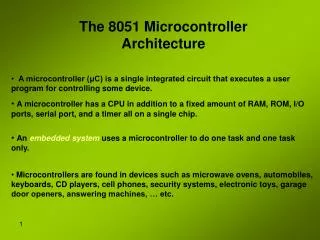
Microcontroller : • A smaller computer • On-chip RAM, ROM, I/O ports... • Example:Motorola’s 6811, Intel’s 8051, Zilog’s Z8 and PIC 16X CPU RAM ROM A single chip Serial COM Port I/O Port Timer Microcontroller
Microprocessor vs. Microcontroller Microprocessor • CPU is stand-alone, RAM, ROM, I/O, timer are separate • designer can decide on the amount of ROM, RAM and I/O ports. • expansive • versatility • general-purpose • Microcontroller • CPU, RAM, ROM, I/O and timer are all on a single chip • fix amount of on-chip ROM, RAM, I/O ports • for applications in which cost, power and space are critical • single-purpose
Embedded System • Embedded system means the processor is embedded into that application. • An embedded product uses a microprocessor or microcontroller to do one task only. • In an embedded system, there is only one application software that is typically burned into ROM. • Example:printer, keyboard, video game player
Three criteria in Choosing a Microcontroller • meeting the computing needs of the task efficiently and cost effectively • speed, the amount of ROM and RAM, the number of I/O ports and timers, size, packaging, power consumption • easy to upgrade • cost per unit • availability of software development tools • assemblers, debuggers, C compilers, emulator, simulator, technical support • wide availability and reliable sources of the microcontrollers.
Block Diagram External interrupts On-chip ROM for program code Timer/Counter Interrupt Control Timer 1 On-chip RAM Counter Inputs Timer 0 CPU Serial Port Bus Control 4 I/O Ports OSC P0 P1 P2 P3 TxD RxD Address/Data
Part 1 Intel 8051: Pin Configurations • Dual In-Line Package • Plastic Lead Chip Carrier • Plastic Quad Flat Pack
Vcc P1.0 1 40 P0.0(AD0) P1.1 2 39 P0.1(AD1) P1.2 3 38 P0.2(AD2) P1.3 4 37 8051 (8031) P0.3(AD3) P1.4 5 36 P0.4(AD4) P1.5 6 35 P0.5(AD5) P1.6 7 34 P0.6(AD6) P1.7 8 33 P0.7(AD7) RST 9 32 (RXD)P3.0 EA/VPP 10 31 (TXD)P3.1 ALE/PROG 11 30 PSEN (INT0)P3.2 12 29 P2.7(A15) 13 28 (INT1)P3.3 (T0)P3.4 P2.6(A14) 14 27 (T1)P3.5 P2.5(A13) 15 26 P2.4(A12) (WR)P3.6 16 25 P2.3(A11) (RD)P3.7 17 24 P2.2(A10) XTAL2 18 23 P2.1(A9) XTAL1 19 22 P2.0(A8) GND 20 21 Pin Description of the 8051
Intel 8051: Pin Configurations • 6 • 1 • 40 • 7 • 39 PQFP • 17 • 29 • 18 • 28 • 1 NIC • 16 P3.4/T0 • 31 P2.7/A15 • 2 P1.0 • 17 P3.5/T1 • 32 PSEN • 3 P1.1 • 18 P3.6/WR • 33 ALE • 4 P1.2 • 19 P3.4/RD • 34 NIC • 5 P1.3 • 20 XTAL2 • 35 EA • 6 P1.4 • 21 XTAL1 • 36 P0.7/AD7 • 7 P1.5 • 22 VSS • 37 P0.6/AD6 • 8 P1.6 • 23 NIC • 38 P0.5/AD5 • 9 P1.7 • 24 P2.0/A8 • 39 P0.4/AD4 • 10 RST • 25 P2.1/A9 • 40 P0.3/AD3 • 11 P3.0/RxD • 26 P2.2/A10 • 41 P0.2/AD2 • 12 NIC • 27 P2.3/A11 • 42 P0.1/AD1 • 13 P3.1/TxD • 28 P2.4/A12 • 43 P0.0/AD0 • 14 P3.2/INT0 • 29 P2.5/A13 • 44 VCC • 15 P3.3/INT1 • 30 P2.6/A14
Pins of 8051(1/4) • Vcc(pin 40): • Vcc provides supply voltage to the chip. • The voltage source is +5V. • GND(pin 20):ground • XTAL1 and XTAL2(pins 19,18)
C2 XTAL2 30pF C1 XTAL1 30pF GND Figure (a). XTAL Connection to 8051 • Using a quartz crystal oscillator • We can observe the frequency on the XTAL2 pin.
Intel 8051: CPU Timing • The internal clock generator defines the sequence of states that make up a machine cycle • A machine cycle consists of 6 states, numbered S1 through S6 • Each state time lasts for two oscillator periods • Each state is then divided into a Phase 1 and Phase 2 half
Pins of I/O Port • The 8051 has four I/O ports • Port 0 (pins 32-39):P0(P0.0~P0.7) • Port 1(pins 1-8):P1(P1.0~P1.7) • Port 2(pins 21-28):P2(P2.0~P2.7) • Port 3(pins 10-17):P3(P3.0~P3.7) • Each port can be used as input or output (bi-direction).
Part 1 Intel 8051: Port Structures • Pseudo bi-directional I/O port structure • For each port pin, there is 1 latch. • When we output the data on ports, it will be written on the latch. • When we input the data from ports, it will be read directly from the port pins. • To use a pin for input latch must be set • To use a pin as outputlatch must be reset
Readlatch Vcc TB2 Load(L1) P1.X pin Internal CPU bus DQ ClkQ P1.X M1 Write to latch TB1 Read pin A Pin of Port 1 P0.x 8051 IC
Read latch Vcc Load(L1) P1.X pin Internal CPU bus DQ ClkQ P1.X M1 Write to latch Read pin Writing “1” to Output Pin P1.X TB2 2. output pin isVcc 1. write a 1 to the pin 1 output 1 0 TB1 8051 IC
Read latch Vcc Load(L1) P1.X pin Internal CPU bus DQ ClkQ P1.X M1 Write to latch Read pin Writing “0” to Output Pin P1.X TB2 2. output pin is ground 1. write a 0 to the pin 0 output 0 1 TB1 8051 IC
Read latch Vcc Load(L1) P1.X pin Internal CPU bus DQ ClkQ P1.X M1 Write to latch Read pin Reading “High” at Input Pin 2. MOV A,P1 external pin=High TB2 • write a 1 to the pin • MOV P1,#0FFH 1 1 0 TB1 3.Read pin=1 Read latch=0 Write to latch=1 8051 IC
Read latch Vcc Load(L1) P1.X pin Internal CPU bus DQ ClkQ P1.X M1 Write to latch Read pin Reading “Low” at Input Pin 2. MOV A,P1 external pin=Low TB2 • write a 1 to the pin • MOV P1,#0FFH 1 0 0 TB1 3. Read pin=1 Read latch=0 Write to latch=1 8051 IC
Other Pins • P1, P2, and P3 have internal pull-up resisters. • P1, P2, and P3 are not open drain. • P0 has no internal pull-up resistors and does not connects to Vcc inside the 8051. • P0 is open drain. • Compare the figures of P1.X and P0.X. • However, for a programmer, it is the same to program P0, P1, P2 and P3. • All the ports upon RESET are configured as output.
Read latch TB2 P0.X pin Internal CPU bus DQ ClkQ P1.X M1 Write to latch TB1 Read pin A Pin of Port 0 P1.x 8051 IC
Vcc 10 K Port 0 P0.0 P0.1 DS5000 8751 8951 P0.2 P0.3 P0.4 P0.5 P0.6 P0.7 Port 0 with Pull-Up Resistors
P3 Bit Function Pin P3.0 RxD 10 P3.1 TxD 11 P3.2 INT0 12 P3.3 INT1 13 P3.4 T0 14 P3.5 T1 15 P3.6 WR 16 P3.7 RD 17 Port 3 Alternate Functions
Pins of 8051(2/4) • RST(pin 9):reset • It is an input pin and is active high(normally low). • The high pulse must be high at least 2 machine cycles. • It is a power-on reset. • Upon applying a high pulse to RST, the microcontroller will reset and all values in registers will be lost. • Reset values of some 8051 registers
Figure (b). Power-On RESET Circuit Vcc + 10 uF 31 EA/VPP X1 30 pF 19 11.0592 MHz 8.2 K X2 18 30 pF RST 9
Pins of 8051(3/4) • EA(pin 31):external access • There is no on-chip ROM in 8031 and 8032 . • The EA pin is connected to GND to indicate the code is stored externally. • PSEN & ALE are used for external ROM. • For 8051, EA pin is connected to Vcc. • “/” means active low. • PSEN(pin 29):program store enable • This is an output pin and is connected to the OE pin of the ROM.
Pins of 8051(4/4) • ALE(pin 30):address latch enable • It is an output pin and is active high. • 8051 port 0 provides both address and data. • The ALE pin is used for de-multiplexing the address and data by connecting to the G pin of the 74LS373 latch. • I/O port pins • The four ports P0, P1, P2, and P3. • Each port uses 8 pins. • All I/O pins are bi-directional.
RESET Value of Some 8051 Registers: Register Reset Value PC 0000 ACC 0000 B 0000 PSW 0000 SP 0007 0000 DPTR RAM are all zero.
A B R0 DPTR DPH DPL R1 R2 PC PC R3 Some 8051 16-bit Register R4 R5 R6 R7 Some 8-bitt Registers of the 8051 Registers
ROM memory map in 8051 family 0000H 0000H 0000H 0FFFH 1FFFH 8751 AT89C51 8752 AT89C52 7FFFH Memory mapping in 8051 4k 8k 32k DS5000-32 from Atmel Corporation from Dallas Semiconductor
7FH Scratch pad RAM 30H 2FH Bit-Addressable RAM 20H 1FH Register Bank 3 18H 17H Register Bank 2 10H 0FH (Stack) Register Bank 1 08H 07H Register Bank 0 00H • RAM memory space allocation in the 8051
7FH Scratch pad RAM 30H 2FH Bit-Addressable RAM 20H 1FH Register Bank 3 18H 17H Register Bank 2 10H 0FH (Stack) Register Bank 1 08H 07H Register Bank 0 00H Stack in the 8051 • The register used to access the stack is called SP (stack pointer) register. • The stack pointer in the 8051 is only 8 bits wide, which means that it can take value 00 to FFH. When 8051 powered up, the SP register contains value 07.
TMOD Register: • Gate : When set, timer only runs while INT(0,1) is high. • C/T : Counter/Timer select bit. • M1 : Mode bit 1. • M0 : Mode bit 0.
TF1: Timer 1 overflow flag. TR1: Timer 1 run control bit. TF0: Timer 0 overflag. TR0: Timer 0 run control bit. IE1: External interrupt 1 edge flag. IT1: External interrupt 1 type flag. IE0: External interrupt 0 edge flag. IT0: External interrupt 0 type flag. TCON Register:
Interrupt Enable Register : • EA : Global enable/disable. • --- : Undefined. • ET2 :Enable Timer 2 interrupt. • ES :Enable Serial port interrupt. • ET1 :Enable Timer 1 interrupt. • EX1 :Enable External 1 interrupt. • ET0 : Enable Timer 0 interrupt. • EX0 : Enable External 0 interrupt.