Instrumentation at Nanostructure Physics, KTH
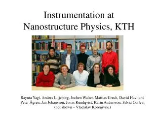
Instrumentation at Nanostructure Physics, KTH. Rayuta Yagi, Anders Liljeborg, Jochen Walter, Mattias Urech, David Haviland Peter Ågren, Jan Johansson, Jonas Rundqvist, Karin Andersson, Silvia Corlevi (not shown – Vladislav Korenivski). Our Realm in Experimental Physics. Low energies ( m eV)

Instrumentation at Nanostructure Physics, KTH
E N D
Presentation Transcript
Instrumentation at Nanostructure Physics, KTH Rayuta Yagi, Anders Liljeborg, Jochen Walter, Mattias Urech, David Haviland Peter Ågren, Jan Johansson, Jonas Rundqvist, Karin Andersson, Silvia Corlevi (not shown – Vladislav Korenivski)
Our Realm in Experimental Physics • Low energies (meV) • Low Temperatures (20 mK) • Small signals (nV, fA) • Single charge (2e=1.3x10⁻¹⁸ C) • Single flux quanta (F0=2.06x10⁻¹⁵ W m2) • Small dimensions (10 – 100 nm)
KTH Nano-Fab Lab Philosophy • Nano and micro scale fabrication,imaging and metrology • Joint laboratory facility, broad user spectrum • Graduate students are users • Low overhead costs, flexible research environment
K. A. Wallenberg Foundation • 9 Msek, 1998 • Electron-beam lithography • Plasma RIE • Wire bonder • clean benches, spinner, microscope, etc. • 10 Msek , 2001 • Atomic Force Microscope • Plasma RIE • Surface profilometer • photo lithography • clean benches
Low Cost (semi) clean room environment Phase 2 Instruments – Phase 1 Instruments Light Microscope Laminar flow benches (spinner, development) Photo Lithography Wet bench, hood Reactive Ion Etcher(s) Surface Profilometer Vacuum Deposition System E-beam lithography Atomic Force Microscope Wire Bonder Fluorescence Microscope Cooled CCD camera
Low cost clean (enough) environment500 – 2000 particles per cubic foot
Ventilated clean air hoodsparticle count < 1/ft.3 after 2 minutes
Electron beam lithography • Versatileresearch tool • Beam writing and SEM capability, 6 inch laser stage. • High resolution (slow, nano features) and Low Resolution (fast, micro structure) Raith Turnkey 150
Thickness measurement 0.1 Å vertical resolution 0.5 mm horizontal Low force (ca. mN?)
Scanning Probe Microscope • Nanoscope IV Multi-mode: • AFM (air, liquid) • STM (air) • MFM, ESFM etc. • Image surface • Force measurement
spin dependant transport in nano-scale junctions(Nanostructure Physics, KTH) Room Temperature Magneto-resistance (MR) Two closely spaced Co/AlOx/Co tunnel junctions
Superconducting nano-circuits as quantum bits(Nanostructure Physics, KTH; Quantum Field Theory, SU) Gate SQUID Au lead SET electrometer Al Tunnel junction
Nanostructured ferroelectrics for linear and nonlinear optics(Laser physics and quantum optics, KTH) Photonic Bandgap Structures ion-exchanged gratings in KTP • = 800 nm, depth > 200 m • aspect ratio > 500:1 • L= 2 mm, w=1mm used as passive narrow band filters Active devices – electrically addressable filters sub-micron periodically domain inverted structures fabricated for first time • = 720 nm, depth 500 m • aspect ratio > 500:1 • L=1 mm, W= 1 mm Top view Bottom view
Nano fabricated X-ray lenses(Biomedical and X-ray Physics, KTH) Compact X-ray Microscope Diffractive Optics -- Zone Plate
Nano-patterned surfaces for cell growth studies(Polymer Chemistry, KTH; Nanostructure Physics, KTH) Electron-microscope image Optical microscope image Sine-wave grooves in PMMA
S-H Protein A cys - biotin - neutravidin fluoro spheres self assemble on nanometer scale pattern(Nanostructure physics, KTH, Protein Engineering, KTH) Neutravidin 40 nm fluorescent sphere 10 mm PEG 50 Å Au 2000 Å
Measurement Equipment • Low Temperatures (down to 20 mk) • High Frequency (up to 2 GHz) • Small Signals (fA, nV, Lockin, low noise AF) • High Impedence (> G Ohm)
Low Temperature Dilution Refrigerator (Tmin 250 mK) He3 Crostat (Tmin 250 mK)
Low Frequency techniques • Lockin Amplifier • Low noise preamplifiers • Home-made based on BB OPA111, high source impedence, high CMR, symmetric baising circuit. • Standford 560 (voltage) and 570 (current) preamps • Noise Matching – match source impedance to input impedence of preamp at given frequency for minimum noise
Network Analyizer up to 2GHz Reflected and transmitted signal, Amplitude and phase • Impedance of high inductance microstrips • Permiability of magnetic films • Characterize transmission lines, couplings, filters No picture - Digital Sampling Oscilloscope with TDR module (ps resolution)
Vibrating Sample Magnetometer M vs. H of this magnetic films Also “loop tracer”, real time rotation in plane of film
Future HF Techniques • ns or sub-ns rise time pulses • Broadband cabling in to cryostat • CW generator greater than 2 GHz • AWF generator • Pulsed RF • Field calculations around microstrips • Tricks …. opto-electric? ……