Download
1 / 38
380 likes | 419 Vues
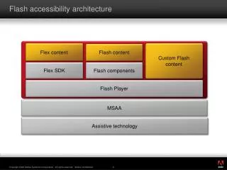
Flash Architecture and Effects. Dave Zeryck. Agenda. The “Rule of Thumb” and where it came from Flash Architecture Flash Write Details Steady-state Flash performance Flash & Write Cache Best Practices/Best Use. The Rule Of Thumb.

E N D
Flash Architecture and Effects Dave Zeryck
Agenda • The “Rule of Thumb” and where it came from • Flash Architecture • Flash Write Details • Steady-state Flash performance • Flash & Write Cache • Best Practices/Best Use
The Rule Of Thumb • Flash Manufacturers say 30K IOPS/Drive, EMC says 2500, why? • YES you can get 30,000 IOPS from one drive under special cases • Very small I/O size • Reads • 2500 IOPS is the expected performance of certain drives under adverse conditions • Flash IOPS vary greatly with several factors • Drive model • Read/Write ratio (writes are slower to process) • IO Size (has a very large impact on IOPS) • Thread count (more requests get more IOPS) • Applications may have to be adjusted to get high IOPS from Flash drives Un-cached IOPS from six spindles, ORION (Oracle) Benchmark
The Rule Of Thumb • What’s behind the Rule of Thumb and Flash behavior? • That’s what we’ll investigate in this presentation • Who is the Rule of Thumb aimed at? • The average user: not performance critical, modest SLA, does not want to ‘architect’ storage • Who is this presentation for? • Those who want, or need, to know just how far you can push the technology • Those who must know how to meet an SLA with the utmost in economy and precision • Understanding Flash drives can help you target their use better • Know your results before you run the workload • Help set expectations with your users • Know which drives will work best for high-priority applications • What we’ll cover in this presentation • Why writes are so different than reads • What differences affect performance between models • How to get the most out of your Flash drives
Buffer w/power backup Parallel IO Channels (16) SLC NAND Flash Dual-ported FC interface Flash Architecture: Anatomy • Flash are a microcontroller-based, complex storage technology • Controller logic to determine location of LBA • Cells are mapped, like a filesystem, not a straight address translation • Buffers writes, holds recent writes and the translation table The Flash Chips are single-level, Enterprise-class, capable of very high write cycles With ‘write leveling’ the drive is warranted for 5 years of continuous use Failure would be gradual, and hidden by the reserved space (next slide)
Flash Architecture: Anatomy • Flash reserve part of the NAND for ‘write leveling’ • A large part of the drive is reserved; amount depends on model • Writes are spread evenly over all cells, over time; any “hot location” (like LUN metadata) will be remapped to less-busy areas • Remapping is done in the background or on-demand • Heavily worn blocks are “retired” to contain rarely-modified pages 2. Writes flush to “ready blocks” 1. Writes hit SDRAM 3. New blocks identified as ready blocks NAND FLASH – total storage 128, 256 or 512 GB SDRAM buffer (hi speed) ‘Worn’ blocks hold rarely accessed data
Flash Architecture: Anatomy • Flash offer true parallel operation, unlike Fibre drives • Up to 16 I/O in parallel • Largest benefit seen in read operations • Applications may have to be modified to maximize Flash performance READS Parallel access up to 16 cells Reads: up to 16 parallel at “unqueued” speed (0.25 ms). 16Concurrent Reads LOGIC Flash Writes: ‘leveling’ operations reduces the parallelism, so queues build (but much slower than on FC) WRITES 16Concurrent Writes LOGIC Flash Some writes will queue, awaiting processing by the mapping layer
Flash Architecture: Anatomy • Flash use a SDRAM buffer which holds: • Index of all pages • Incoming writes • Incoming writes buffered • Incoming writes are gathered into “blocks”, status returned immediately • Blocks are written to the NAND asynchronously Buffer (SDRAM) Flash NAND ChipsSelf-identifying data arranged in pages Index: map of all LBA locations Metadata User data New Writes
Flash Architecture: Anatomy • Flash Resiliency • Power capacitors maintain power to the buffer in the event of a system power failure • Contents are written to the persistent store (flash) if power fails • Index table is backed up to flash when powered down. • On power up, the table is reloaded into SDRAM and a consistency check is run. • If the table is found to be inconsistent, the table is rebuilt. This is done by reading all of the flash metadata and reconstructing the data. All of the flash data is self identifying. On power fail, all data is secured to persistent Flash Buffer (SDRAM) Flash NAND ChipsSelf-identifying data arranged in pages Index: map of all LBA locations Metadata User data New Writes
Flash Architecture: Pages (Flash = CX Cache ops) • Architecture of an Flash affects the operation • Cells are addressed by pages, currently 4 - 16 KB • 73, 200 GB drives use 4 KB pages • 400 GB drives have 16 KB pages • Page contents are a contiguous address space, like SP cache pages • Like an SP Cache page, small IO will be held within 1 page • UNLIKE an SP cache page, LIKE a disk sector, the entire page must be valid before writing • Like a disk sector, the page is the smallest size the Flash can write to NAND • The Flash cannot write a partial page to the NAND chip Two 2 KB I/O in a 4 KB Flash page; must be contiguous WRT LBA 4 KB I/O in a 4 KB Flash page LBA 0x0400 LBA 0x13FF LBA 0x1400 LBA 0x23FF
Flash Architecture: Blocks • Pages are grouped together into blocks of 128 to 256 KB • NOT to be confused with: • SCSI “block” which is a sector on a HDD • Filesystem block/page • Multiple pages in a block “jumbled” together • The addresses of pages in a block do not have to be contiguous • Block Images are held in buffer until the block is full, then written to an erased block on disk • Writes to NAND are (preferred) full-block writes Logical map of pages Page: 4 KB or 16 KB Block: 256 KB The pages in this block can be from random locations in the LBA map; the Flash keeps a map of each page, its location in the Flash and the LBA it corresponds to LBA 0x0400 LBA 0x2400 LBA 0x4400 LBA 0x6400
Flash Architecture: Blocks • Writes to NAND are done at the block level • The drive prefers to wait until a block is full but it does not have to The entire block is written to an erased block on the Flash chips Block, in buffer Blocks, on NAND Page: 4 KB or 16 KB
Flash Architecture: Channels and devices • Channels are paths to physical devices (chips) • Flash drives have multiple channels: discrete devices can be read from or written to simultaneously • Large I/O is striped across the channels • So, parts of a large I/O are split between multiple blocks A Block Image is written to a specific channel, to a separate NAND chip Host I/O 512 KBwrite Block Image: 256 KBx 2 (in drive buffer) Buffer Channel NAND Channel1 Chip1 . . . Channel2 Chip2 ChannelX ChipX
Legend Valid Invalid Erased Flash Architecture: Page States • Page States • Valid page: page contains good data (referenced by host and Flash) • Invalid page: page contains ‘stale’ data. One of: • Overwritten in the host filesystem • Moved/coalesced by the Flash itself • Erased: pages in an erased block; the block is not in use • A block has pages that are a or combination of valid and invalid, all erased, and sometimes a mix of valid, invalid and erased Flash Block on drive Block1 LBA 0x2A1 Logical view on host A small file (8 KB) 2 filesystem blocks of 4 KB each LBA 0x040 LBA 0xCF0 LBA 0x040 The 8 KB of file data fits in 2 pages of 4 KB each LBA 0x240 LBA 0x0FA LBA 0x240
Legend Valid Invalid Erased Flash Architecture: Page States SDRAM NAND • How a page becomes invalid • Overwritten by host, the new value is stored in a page in SDRAM buffer (block image) • The old page in NAND is marked invalid Block image (Buffer) Block On Chip LBA 0x2A1 Logical view on host EXAMPLE: Step 1, host overwrites existing filesystem page LBA 0x040 0x040 New LBA 0x040 LBA 0xCF0 LBA 0x240 LBA 0x0FA LBA 0x240
Legend Valid Invalid Erased Flash Architecture: Page States SDRAM NAND • How a page becomes invalid • Overwritten by host, the new value is stored in a page in SDRAM buffer (block image) • The old page in NAND is marked invalid Block image (buffer) 0x040 New Block On Chip LBA 0x2A1 Logical view on host EXAMPLE: Step 2, Flash drive stores data in a block image in the drive’s buffer LBA 0x040 0x040 New LBA 0xCF0 LBA 0x240 LBA 0x0FA LBA 0x240
Legend Valid Invalid Erased Flash Architecture: Page States SDRAM NAND • How a page becomes invalid • Overwritten by host, the new value is stored in a page in SDRAM buffer (block image) • The old page in NAND is marked invalid Block image (Buffer) 0x040 New Block On Chip LBA 0x2A1 EXAMPLE: Step 3, Flash invalidates old block on chip by setting a bit in the mapping database; at some point the new block image in buffer is written to chip in a different block Logical view on host Data is left in place, but reference removed in index 0x040 New LBA 0xCF0 LBA 0x240 LBA 0x0FA LBA 0x240
Legend Valid Invalid Erased Flash Architecture: Reserve Capacity • Some percentage of the drive’s capacity is reserved • It is not included in the “user addressable” capacity • HOWEVER – this capacity will be used • This capacity will be used even if the user does not address the full addressable capacity • We will take a simple example – “4 MB Flash Drive” • Flash ‘example’ has 16 blocks addressable, 16 blocks reserve • 1 block = 256 KB; 16 blocks = 4 MB • User binds 4 MB LUN - consumes all addressable blocks • User writes to only 1 MB, but does so randomly Addressable capacity Reserve Blocks Example Flash: 4 MB addressable; state new drive,before LUNs bound
Legend Valid Invalid Erased Flash Architecture: Reserve Capacity Addressable capacity Reserve Blocks Example Flash: 4 MB LUN bound All blocks of addressable capacity have been written by zero process Addressable capacity Reserve Blocks User writes 1 MB Flash writes to erased blocks in reserve, invalidates existing blocks User overwrites thesame 1 MB address Flash again uses erased blocks in reserve
Flash Architecture: Reserve Capacity Addressable capacity Reserve Blocks User overwrites thesame 1 MB addresses 2 more times Before any additional data is written, some blocks on disk must be erased
Legend Valid Invalid Erased Flash Architecture: Reserve Capacity • What about random access? If random writes are made, over time all blocks will end up with some amount of valid and invalid pages
Flash Write Details • Operation • Blocks are assembled in the Flash DRAM buffer and written in a single operation • Flash can write a partial block but avoids this if possible • Issue 1: Backfill • When writing a block, for all pages in the block, the entire page must be written • A block receiving I/O smaller than the page must ‘backfill’ the contents of the page from the existing locale in the Flash • Issue 2: Block erasing and consolidation • Flash can only write to erased locations • A “block” is the smallest structure that can be erased in a NAND-flash device • Issue 3: Large IO • Writing large I/O takes longer than smaller IO • Issue 4: Reserve Space • More reserve space (as a % of capacity) will affect performance
Read existing page Flash Write Details: Backfill • Issue 1: Small writes and Backfill • Writing an I/O smaller than 1 page requires read-modify-write • The existing page on the Flash chip must be read into SDRAM • Once read the old page will be invalidated, as the new page will contain the current (merged) version of the data Block image in disk buffer w/ 16K pages (only 8 pages shown) Existing Page on Chip: 16 KB Write: 8 KB Existing page on chip is invalidated Page complete in buffer
Flash Write Details: Backfill • Issue 1: Small writes and Backfill • Writing an I/O smaller than 1 page results in more work for back end • The Flash must write the new data plus the back fill data to the NAND • Also, erased blocks are used up much faster (since the drive must write 2X of incoming load) Example, 8 KB to 16 KB page: 16 * 8KB = 128 KB written by Flare, 256 KB written to NAND Block in Flash DRAM Buffer (16 KB pages) Writes: 8 KB Legend Old data backfilled from chip New data written from host 16-KB page
Flash Write Details: Block erasing and consolidation • Issue 2: Erasing Blocks • It can write as little as a single page but avoids that operation • The smallest structure you can erase in a NAND flash device is a block • The Flash logic minimizes erase operations when processing incoming I/O • On a new drive, the SSD controller will write to every block on the drive before erasing any blocks • This is true even if only a small portion of the drive is being written • The Flash attempts to erase blocks during ‘idle’ periods when incoming I/O is at a low rate • To be erased, every valid page in a block must first be written to another block Example: Two sparse blocks being consolidated (housekeeping) 1. Read valid pages into buffer Note: We are only showing 16 pages in each block to keep the graphics a reasonable size Buffer NAND
Flash Write Details: Block erasing and consolidation • Issue 2: Erasing Blocks • It can write as little as a single page but avoids that operation • The smallest structure you can erase in a NAND flash device is a block (128 KB) • The Flash logic minimizes erase operations when processing incoming I/O • On a new drive, the SSD controller will write to every block on the drive before erasing any blocks • This is true even if only a small portion of the drive is being written • The Flash attempts to erase blocks during ‘idle’ periods when incoming I/O is at a low rate • To be erased, every valid page in a block must first be written to another block Example: Two sparse blocks being consolidated (housekeeping) 2. Erase blocks on chip 3. Write consolidated block to chip Buffer NAND
Write Page Write Page Flash Write Details: Large Writes (REDO) • Issue 3: Large writes (BE queue issues) • Writes larger than the page size are mapped to more than one block • The multiple writing of blocks does not appear to be in parallel • Large write IO is noticeably slower than small I/O • This is noticeable from 4 ->8->16->32->64 KB etc. • We do not know the exact mechanism, but there may be a write queue from the SDRAM buffer Blocks in disk buffer Pages: 4 KB Write: 8 KB
Reserve Space • Issue 4: Reserve Space • The amount of reserve space affects write response time (SUSTAINED) • For a given amount of capacity, if you reduce reserved space, each block will have, on average, more valid pages • If blocks have a high % of valid pages, it is more difficult to coalesce and erase a block • This is an exponential curve • The 73 GB drive has about 43% reserved, the 400 GB has about 22% reserved • Thus, the 400 GB drive, when fully dirtied, will work about 2.5 times as hard to process writes • You can achieve the same effect by “short stroking” the 400 GB drive to 300 GB • If only 300 GB are bound to LUNs the 400 GB drive has much more reserve space Case 1: 50% reserve capacity Each block averages 50% valid pages Read only 2 blocks into buffer to free 1 block Case 2: 20% reserve capacity Each block averages 80% valid pages Read 5 blocks into buffer to free 1 block
Steady state and consolidation • Steady-state performance is what we see when all blocks (including reserve blocks) on an Flash have some valid data written to them • GIVEN WHAT WE KNOW about how Flash drives process writes, we can expect variations in performance • A drive with fewer reserve blocks will take longer and use more cycles to erase blocks in order to take incoming writes • A drive with pages larger than I/O write sizes will be more fragmented and take more cycles to process writes than drives with cache page equal to or less than write size • The 400 GB drive has both a large cache page (16 KB) and far less reserve space (as measured by % of capacity) • The drive will consolidate blocks when idle in order to avoid coalescing bottlenecks when busy Disk at steady-state: every block has some amount of data in it, it is fragmented, and blocks can only be erased by copying two or more blocks into the buffer and coalescing them
Data1 Data2 Data3 Data4 Parity Parity Flash and Write Cache • Original Guidance: “Flash does not need cache” • Conservative: avoid side effects from full cache • New guidance: “Flash can be cached in many cases” • Experience: many uses of Flash + Cache in the field • No major problems encountered • Practical: Write Cache offers many benefits • Allows consolidation of I/O (Necessary for LOG files) • Improves response time for writes (RAID 5 common with EFD, 4 operations) Processor memory Host writessequentially Data1 Data2 Data3 Data4 RAID5 Stripe
Best Practices • Our goal is to show the best potential for the drives • There is no load which will break the drive, or overheat it, or tire it out • The following slides have two themes: Best Use, and OK to Use • Best use are those applications that get the maximum performance advantage from the drives • High read rates • Smaller IO • IO Patterns that are not optimal for cached FC implementations • Why spend Flash prices for IO that FC + Flare Cache handle just fine? • OK to Use are profiles that will do just fine with Flash, but: • Cached FC could do it as well • Do not give you the big “Flash advantage” you might expect
Small footprint, big effect Best Practices: Best Use • Databases (most common use of Flash) 4 to 15 Flash drives typical • Indexes and busy tables: “10% of the table spaces that do 80% of all I/O” • TEMP space • BUT – turn ON write cache • Biggest disk-for-disk increase in read-heavy tables (10 – 20X) • Some clients using Flash for write-heavy tables • Use write cache for better response time • Flash flushes cache faster, better results for other (FC-based) tables as well. Before: disks busy, cache full, some I/O waiting on cache After: disks less busy, cache flushes faster to Flash and FC as well Write Cache (90%) Write Cache (40%) All FC drives are busy FC drive queues lower Flash for the heavy writers
Best Practices: Best Use • Really Big Databases are a little different • We see up to 30 Flash in larger DBs • Some users have write caching OFF for Flash – to maximize write throughput • Oracle ASM 11gR2 • An ASM instance can be presented with different ASM disk groups (pools) • The user can designate a group as FAST, AVERAGE or SLOW. • We suggest you designate Flash as “FAST” Before: all writes mirrored, SP & cache busy After: Busy tables to UNCACHED Flash drives: less mirror traffic, better response time Heavy cache mirroring Reduced cache mirroring SPA SPB SPA SPB FC drives need write cache FC drives cached, Flash uncached
Small footprint, big effect Best Practices: Best Use • Messaging (Exchange, Notes) benefits from the same effect • Move some of the databases to Flash, and all users benefit • Use RAID 5 for Exchange on Flash • Turn on write cache • Writes flush to RAID 5 on Flash faster than RAID 1/0 on FC • Reads are likely better distributed than from RAID 1/0 on Flash • Flash rebuilds faster than FC and impact is less Before: disks busy, cache full, some I/O waiting on cache After: disks less busy, cache flushes faster to Flash and FC as well Write Cache (90%) Write Cache (40%) All FC drives are busy FC drive queues lower Flash for the heavy writers
Best Practices: OK to Use – but why? • Databases: • Oracle Flash Recovery. NOTE – SATA do fine here, more economical • Redo logs. BUT – FC is sufficient, less cost • Turn Write Cache ON for Redo LUNs, even if Redos are on Flash • Archive Logs. However, FC, even SATA do fine here • Media: Mostly FC used here • Editing configurations are the best fit from media for Flash • Flash is very quick to serve the small metadata operations • Some advantage to using Flash with multistream access • Large reads and writes in parallel (sharing disks among streams) does not suffer from “disk seek inflation” as seen on rotating media • FC will still give more predictable write performance at a micro level, due to Flash’s internal structure • Any time power/cooling issues are #1
Best Practices: Flash and Write Cache • Original guidance was no write cache with Flash drives • Flash is fast even without it • We did not want Flash LUNS to hit force flushes in cache • Extensive field use shows Flash + DRAM Cache is very effective • No pathological cases encountered, due to conservative guidance • Please avoid heavy writes to SATA when using write cache and Flash • DRAM Cache is very effective with Flash Drives • Write Caching of sequential writes, to optimize RAID 5 updates • Faster response time of small writes
Summary • Flash drives are revolutionary: truly random access storage, so different behavior • There are implementation details to flash that make them behave differently as well • Writes take time to absorb • Any mix of reads and writes will slow overall performance • System write cache is effective with Flash drives • Best practices use cache with some applications, not with others • Fit the solution to the problem