Download
1 / 6
60 likes | 69 Vues
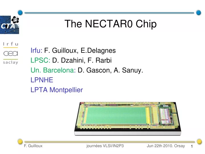
The NECTAR0 Chip Irfu: F. Guilloux, E.Delagnes LPSC: D. Dzahini, F. Rarbi Un. Barcelona : D. Gascon, A. Sanuy. LPNHE LPTA Montpellier. Nectar: New Electronics for the Cerenkov Telescope ARray. Goal: perform the readout of the photodetectors of the telescopes of the future CTA.

E N D
The NECTAR0 Chip Irfu: F. Guilloux, E.Delagnes LPSC: D. Dzahini, F. Rarbi Un. Barcelona: D. Gascon, A. Sanuy. LPNHE LPTA Montpellier
Nectar: New Electronics for the Cerenkov Telescope ARray • Goal: perform the readout of the photodetectors of the telescopes of the future CTA. • CTA: “convergence” of the HESS, Magic and probably Veritas communities • ~ 100 telescopes of 3 different geometries, with ~1000 pixel camera • Very high background => need for very fast camera (<10ns integration time required ). • Electronics located at the focal plane of the telescope: need for high dynamic range low power, integrated electronics • Performance of fast analogue memories perfectly matches with the requirements: • ARS0 => HESS, SAM => HESS-2. • Nectar: Same concept + integrated ADC => ANR grant. HESS(2) Namibia Magic: Canary islands
Use of Analogue memory on NECTAR. • Used as a circular buffer with area of interest readout • ~“Cut & Paste” of the SAM analogue memory (2 differential channels) • Extended to 1024 cells/ ch (instead of 256) to deal with longer trigger latency
NECTAR0 block diagram Collaboration with Barcelona Univ. (High Slew Rate/low power Amp) 12-bit ADC (IP from LPSC)
Integration of the ADC IP. • Use of an IP block designed by IN2P3/LPSC shared between 2 channels. • See “A low power 12-bit and 25-MS/s pipelined ADC for the ILC / Ecal integrated readout”, F. Rarbi, D. Dzahini, L. Gallin-Martel”, 2008, IEEE NSS. • Preferred to Wilkinson architecture originally proposed for simplicity of use. • Good performances reported, power pulsing available. Quasi-static use possible. • Practically: • Full “flat” layout provided by LPSC. “coded” netlist, for simulation (no schematic). • Use of the IP not so obvious & required more time than foreseen. • Simulations made using extracted view from DIVA. Were absolutely necessary for checking (timing, ranges,…) • Direct contact with LPSC (very available) was necessary . • Full chip DRC/LVS with ASSURA in macro mode: quite tricky to use. Solution found only few days before submission.
Nectar 0 chip Submission • CMOS AMS 0.35µm technology: 3x7mm chip. • TQFP 128 (0.4mm pitch) package. • Submitted in an engineering run common with IPHC • Return expected in end of June 2010. • Tests will take place in the “new” labs of Jussieu. Digital LVDS SCA Input buffers ADC RO + MUX