Download
1 / 12
120 likes | 266 Vues
Total Dose Response of HfSiON MOS Capacitors. D. K. Chen, F. E. Mamouni, R. D. Schrimpf, D. M. Fleetwood, and K. F. Galloway Department of Electrical Engineering and Computer Science, Vanderbilt University, Nashville, TN. G. Lucovsky and S. Lee Dept of Physics and Material Science,

E N D
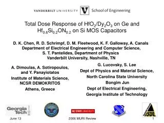
Total Dose Response of HfSiON MOS Capacitors D. K. Chen, F. E. Mamouni, R. D. Schrimpf, D. M. Fleetwood, and K. F. Galloway Department of Electrical Engineering and Computer Science, Vanderbilt University, Nashville, TN G. Lucovsky and S. Lee Dept of Physics and Material Science, North Carolina State University B. Jun and J. D. Cressler Dept of Electrical Engineering and Computer Science, Georgia Institute of Technology
Introduction • Quantum mechanical tunneling significant in SiO2 • Charge trapping in HfSiON (Amorphous and Crystalline HfO2) [G. Lucovsky et al., IEEE Trans. Nucl. Sci., vol. 53, pp. 3644-3648, 2006.] • Total dose irradiation and constant voltage stress • TID-induced charge trapping compared to previous Hf silicate devices
Vg Al Gate HfSiON FOX FOX SiON Silicon Substrate Al Substrate Contact Device Description • (HfO2)0.4(SiO2)0.4(Si3N4)0.2 Low-Si3N4 K = 14.6 tox = 15 nm • (HfO2)0.3(SiO2)0.3(Si3N4)0.4 High-Si3N4 K = 12.7 tox = 13 nm • Equivalent oxide thickness ~ 4 nm • The samples were prepared by remote plasma enhanced chemical vapor deposition (RPECVD), with ~0.6 nm SiON layer; Rapid thermal anneal done at 900 oC
Experimental Details • 1-MHz C-V measurement at a rate of 0.05 V/s; Irradiated with 10 keV X-ray at a rate of 31.5 krad(SiO2)/min • Interface trapped charge density (Nit) unchanged after radiation; prerad Nit ~ 3.8 x 1012 cm-2 • Relatively small gate leakage current (<10 pA @ Vfb + 1 V) unaffected by radiation
Improvement Relative to Hf Silicate Devices • TID-induced charge trapping factor of 17 less relative to previous Hf silicate devices [J. A. Felix et al., IEEE Trans. Nucl. Sci., vol. 49, pp. 3191-3196, 2002]
Midgap Voltage Shifts • Weak bias dependence • Relative low mobility of holes in HfSiON similar to hafnium silicates [J. A. Felix et al., IEEE Trans. Nucl. Sci., vol. 49, pp. 3191-3196, 2002] • Electron trapping • TID-induced and substrate injection at large positive biases
Comparison of Low- and High-Si3N4 Devices • Crystalline HfO2 in the low-Si3N4 film contains grain boundaries • Negative gate bias show similar charge trapping levels
Constant Voltage Stress (Substrate Injection) • O vacancies and interstitials in the Low-Si3N4 film favorable for electron trapping from substrate injection • Defects located near the interface an important source for electron trap sites
Constant Voltage Stress (Gate Injection) • Level of charge trapping much less compared to substrate injection • Saturation occurs much earlier than substrate injection case • Electron injection from the gate and movement of charge centroid
Comparison to Hf Silicate Devices • Electron injection balances positive charge trapping for positive and negative biases • ∆Not ~ factor of 17 smaller at 1 Mrad(SiO2) • 1.2 x 1012 cm-2 Hf silicate • 7.1 x 1010 cm-2 HfSiON • Reduced charge trapping indicates superior HfSiON film qualities (smaller bulk trap density) and improvements in processing
Conclusions • HfSiON show drastic improvements in total dose irradiation hardness relative to Hf silicate devices • Crystallization creates grain boundary defects especially vulnerable to stress-induced electron trapping • Reduced charge trapping indicates smaller bulk defect density in HfSiON film relative to Hf silicates
Acknowledgements • Dr. Lucovsky’s group at NC State University for providing the samples • Air Force Office of Scientific Research (AFOSR) for supporting this work