High Brightness Electron Source Development
Explore cutting-edge diagnostic techniques for high brightness electron sources, including Auger Spectroscopy, LEED, photoreflectance, and electron energy analyzers. Learn about response time measurements, work function measurement, and XRF in the development of GaAs(Cs,F) and Alkali-Antimonide photocathodes. Discover the latest advancements in DC gun development and photocathode diagnostics for brightness optimization. Presented at the DOE Contractors' Meeting in 2011.

High Brightness Electron Source Development
E N D
Presentation Transcript
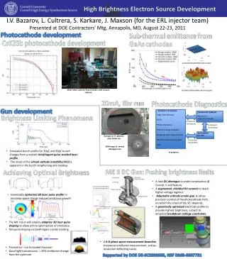
High Brightness Electron Source Development DIAGNOSTIC TECHNIQUES PREPARATION CHAMBERS • Auger Spectroscopy • LEED • Photoreflectance • Electron Energy Analyzers • Response time measurements • Work function measurement • XRF • …. • GaAs(Cs,F) • Alkali-Antimonide I.V. Bazarov, L. Cultrera, S. Karkare, J. Maxson (for the ERL injector team) Presented at DOE Contractors’ Mtg, Annapolis, MD, August 22-23, 2011 Crater Light gray ~1.5 mm diameter Photocathode film Sub-thermal emittance from GaAs cathodes • ERL INJECTOR • DC GUN Photocathode development Brown colored area ~4 mm diameter ~0.5 mm gap CsK2Sb photocathode development Brightness Limiting Phenomena Multi-Alkali Cathode Prep-chamber with vacuum suitcase Photocathode Diagnostics • Simulated bunch profile for 20pC and 80pC bunch charges from a realistic birefringentpulse-stacked laser profile. • The onset of the virtual cathode instability (VCI) is apparent in the bunch lengthening and breakup. 20mA, 8hr run Gun development In Vacuum Connection In Vacuum Connection Damage on Si substrate after 20mA run In Vacuum Connection MK II DC Gun: Pushing brightness limits In progress… SEM image of central damaged area • A new DC photogunis under construction @ Cornell. It will feature: • A segmented, shielded HV ceramic to reach higher voltage regimes. • Adjustable cathode-anode gap, to allow precision control of the photocathode field, on which the onset of the VCI depends. • A genetically optimized electrode profile to provide highest brightness, subject to empirical breakdown voltageconstraints. Achieving Optimal Brightness Use of Genetic Algorithms to optimize gun geometry • Genetically optimized 3D laser pulse profile to minimize space charge induced emittance growth. Varying Pierce angle (0 to 45) • The MK II Gun will employ adaptive 3D laser pulse shapingto allow online optimization of emittance. • Temporal shaping via birefringent crystal stacking • Transverse – via truncated Gaussian • Good light transmission, < 20% emittance change from the optimum Varying gap (2 to 12 cm) • A 6-D phase space measurement beamline, transverse emittance measurement, and ps-resolution deflecting cavity. Supported by DOE DE-SC0003965, NSF DMR-0807731