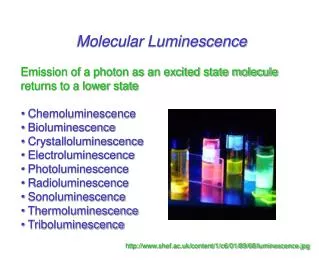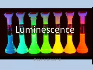
Luminescence
5. Luminescence. 5.1 Light emission in solids 5.2 Interband luminescence 5.3 Photoluminescence 5.4 Electroluminescence. 5.1 Light emission in solids. The spontaneous emission rate for a two level:. The reverse process of absorption – emission

Luminescence
E N D
Presentation Transcript
5 Luminescence 5.1 Light emission in solids 5.2 Interband luminescence 5.3 Photoluminescence 5.4 Electroluminescence
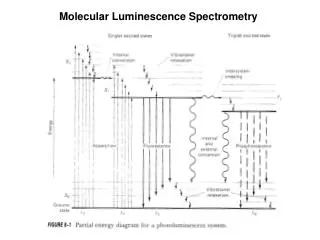
5.1 Light emission in solids The spontaneous emission rate for a two level: • The reverse process of absorption – emission • Emission in solids is called luminescence. • Luminescence mechanisms: • Photoluminescence (PL) • Electroluminescence (EL) A: Einstein A coefficient; R=A-1: radiative lifetime of the transition. • The transition have large absorption coefficients • also have high emission probabilities and short • radiative lifetime; • Upper level is populated. • In normal circumstances the electrons relax to within ~ kB T of the bottom of excited state band. The holes follow a similar series of relaxations. Thus light is only emitted within a narrow energy range. • Non-radiative relaxation: The excited energy may transfer into heat by emitting phonons or be trapped by defect. Electrons are injected into the excited state band and relax to the lowest available level. The photon is emitted when an electron in an excited state drops down into an empty state in the ground state band. These empty state are generated by the injection of holes.
5.1 Light emission in solids 5.2 Interband luminescence Total rate: The interband luminescence corresponds to annihilation of an electron-hole pair (electron-hole recombination) 5.2.1 Direct gap materials The luminescent efficiency R: If R<< NR, R 1, maximum possible amount of light is emitted. If R >> NR, R 0, light emission is very inefficient. The efficient luminescence requires that the radiative lifetime should be much shorter than the non-radiative lifetime The luminescent intensity at frequency : The injected electrons and holes relax very rapidly to lowest energy states. The photons are emitted when electrons at the bottom of the conduction band recombine with holes at the top of the valence band. The typical values of R is in the range 10-8– 10-9 s. The transition should be dipole allowed and have large matrix elements and the same k vector (near k=0, thus close to h=Eg).
The PL was excited by absorption of 4.9 eV photons from a frequency doubled copper vapour laser. The spectrum consist of a narrow emission line at 3.5 eV close to the band gap energy, while the absorption shows the usual threshold at Eg with continuous absorption for h > Eg. The interband luminesence in an indirect gap material is a second-order process. The R much more longer than for direct transition, therefore this makes the luminescence efficiency small. So the indirect gap materials such as silicon and germanium are generally band light emitters. 5.2.2 Indirect gap materials In an indirect materials, conservation of momen- tum requires that a phonon must either be emitted or absorbed when the photon is emitted.
The total number density Ne of electrons: 5.3 Photoluminescence 5.3.1 Excitation and relaxation The density of state in conduction band: Fermi-Dirac distribution for the electrons: (The system is in a situation of quasi- equili- brium, thus is no unique Fermi energy. E=0 corresponds to the bottom of the conduction band or the top of the valence band) ( a) Schematic diagram of the processes occurring during PL in a direct gap semiconductor after excitation at frequency L. The electrons and holes rapidly relax to the bottom of their bands by phonon emission (~10-13s) before recombining by emitting a photon ( ~ 10-9s). (b) Density of states and level occupancies for the electrons and holes after optical excitation. The distribution functions shown by the shading apply to the classical limit where Boltzmann statistics are valid. The total number density Ne of holes: These two Eqs can be used to calcuulate
5.3.2 Low carrier densities At low carrier densities, the occupancy of the levels is small and +1 factor in fe(E) cab be ignored. The electron and hole distribution will be described by classical situation. Fermi Boltzmann distribution : (valid at low densities and high temperature) PL spectrum of GaAs at 100 K. The excitation source was a helium neon laser operating at 632.8 nm (1.96 eV) . The spectrum shows a sharp rise at Eg due to the (h - Eg)1/2 factor and then falls off exponentially due to the Boltzmann factor. The full width at half maximum of the emission line is very close to ~ kBT The inset give a semi-logarithmic plot of the same data.
Ai high carrier densities, the electron and hole distributions are described using Fermi-Dirac statistics. This situation is called degeneracy: In the extreme limit of T = 0 Electron-hole recombination can occur between any states in two bands, therefore there is a broad emission spectrum stating at Eg up to a sharp cut-off at . As finite temperature, the cut off at will be broadened over an energy range ~kBT. 5.3.3 Degeneracy Time-resolved PL spectra of Ga0.47In0.53As at lattice temperature TL=10 K. The sample was excited with laser polse at 610 nm with an energy of 6 nJ and a duration of 8 ps. This generated an initial carrier density of 21024m-3.
5.3.4 Photoluminescence spectroscopy Photoluminescence (PL) spectra: The sample is excited with a laser or lamp with photon energy greater than the band gap. The spectrum is obtained by recording the emission as a function of wavelength. Photoluminescence excitation spectroscopy (PLE): The detection wavelength is fixed and the excitation wavelength is scanned. The technique allows the absorption spectrum to be measured because the signal strength is simply proportional to the carrier density, and in turn is determined by absorption coefficient. Time-resolved photoluminescence spectroscopy: The sample is excited with a very short light pulse and the emission spectrum is recorded as a function of time after the pulse arrives. The time-dependence of the emission spectrum gives direct information about the carrier relaxation and recombination mechanisms, and allows the radiative lifetime to be measured.
5.4 Electroluminescence • Light emitting diodes (LEDs) • Laser diodes (LDs) 5.4.1 General principles of electroluminescence devices The microscopic mechanisms that determine the emission spectrum of EL are exactly the same as the ones of PL. The only difference is that the carriers are injected electrically rather than optically. (~ 1m) (~ 500 m) Active region (~ mm) Layer structure (a) and circuit diagram(b) for a typical EL device. The thin active region at the junction of the p- and n-layer is not shown
5.4.1 General principles of electroluminescence devices • The main factors that determine the choice of the material: • (1) The size of the band gap: Eg ; kBT ; • Constraints relating to lattice matching; • the ease of p-trpe doping. • Two groups: • i) arsenic(As) and phosphorous(P) compounds: • GaAs: 870 nm, AlxGa1-xAs: 630-870 nm • (local area fibre networks (850 nm) and LED) • problem: become indirect as Eg gets larger. • GaxIn1-xAsyP1-y: 920-1650 nm (optics industry). • ii) nitride (N) compound: • GaN: 3.4 eV at RT; InN: 1.9 eV at RT • alloy of GaN and InN: 360 – 650 nm (2) Grow thin ultra-pure layers on the top of a substrate by epitaxy: • liquid phase epitaxy (LPE) (m); • metal-organic vapour phase epitaxy • (MOVPE); • metal-organic chemical vapour phase • deposition (MOCVD); • molecular beam epitaxy (MBE). Band gap of selected III-V semiconductors used for marking LEDs and LDs. as a function of their lattice constant. • Wide band gap semiconductors have very • deep acceptor levels, thus is difficult in doping. • discovering new technique.
5.4.2 Light emitting diodes Grow thin ultra-pure layers on the top of a substrate by epitaxy. Semiconductor ergenning Fig4.1 The diode consist of a p-n diode with heavily doped p and n regions. Band diagram of a light emitting diode at (a) zero bias, and (b) forward bias V0 Eg/e. The bias is applied to drive a current, shift the EF and shrink the depletion region. This creates a region at the junction where both electrons and holes are present. Light is emitted when the electrons recombine with holes in the region. EL spectrum of a GaAs LED at RT. This gives emission in the near- IR around 870 nm. The full width at half maximum of the emission line is 58 mV, which is about twice kBT at 293 K.
5.4.3 Diode lasers Superior performance in output efficiency, spectrum linewidth, beam quality and response speed. Derived from the equilibrium condition, can be apply in all other cases as well. In normal conditions: N1 > N2; In laser oscillation: N2 > N1 (population inversion) The principle of LD: The top of valence band is empty of electrons, while the bottom of the con- duction band is filled with electrons. There is population inversion at the band gap frequency Eg/e. This gives rise to net optical gain. Laser can be obtained if an optical cavity(R1>>R2) from the end faces of gain medium is provided. Fig B.2 • Absorption, spontaneous emission and stimulated emissions between two levels of an atom in the presence of electromagnetric radiation with energy density u(v). • Spontaneous emission: • Absorption transition: • Stimulated emission: Steady state condition: Relationship of A and B coefficients:
5.4.3 Diode lasers (1) Frequency and line width: The resonant longitudinal mode condition: l = integer /2n The resonant frequency: v = integer c/2nl The best laser are single longitudinal mode with emission line widths in the MHz range. (2) Gain and threshold value: gain coefficient: Intensity: Stable oscillation condition at a round-trip in the cavity: (3) Out power and slope efficiency: • : quantum efficiency defined the fraction of injected electron-hole pairs that generate photons. in increases linearly with the injection current Iin, once the laser is oscillating the gain is clamped at the value of th , otherwise the gain would exceed the losses, and the stability condition would not hold. For Iin > Ith, the extra electrons and holes cause the output power to increase. slope efficiency = 1, slope efficiency = hv/e.
5.4.3 Diode lasers Schematic diagram of an oxideconfined GaAs- AlGaAs heterojunction stripe laser. The current flows in the –z direction, while the light propagates in the x direction. The stripe is defined by the gap in the insulating oxide layers deposited on the top of the device during the fabrication process. The active region is the intrinsic GaAs layer at the junction between the n- and p-type AlGaAs cladding layers • Exercises: • The band gap of the III-V semiconductor alloy AlxGa1-xAs at k=0 varies with composition according to Eg(x)=(1.420+1.087x+0.438x2)eV. The material is direct for x 0.43, and indirect for larger values of x. Light emitters for specific wavelengths can be appropriate choice of the composition. • (i). Calculate the composition of the alloy in a device emitting at 800 nm. • (ii). Calculate the range of wavelengths than can usefully be obtained from an AlGaAs emitter. • 2. A very short laser pulse at 780 nm is incident on a thick crystal which has an absorption coefficient of 1.5106 m-1 at this wavelength. The pulse has an energy of 10 nJ and is focused to a circular spot of radius 100 m. • (i) Calculate the initial carrier density at the front of the sample.
(ii) If the radiative and non-radiative lifetimes of the sample are 1 ns and 8 ns respectively, calculate the time taken for the carrier density to drop to 50 % of the initial value. (iii) Calculate the total number of luminescent photons generated by each laser pulse. 3. Explain why the emission probability for an interband transition is proportional to the product of the electron and hole occupancy factors fe and fh respectively. In the classical limit where Boltzmann statistics apply, show that the product fefh is proportional to exp(-(hv –Eg)/kBT).