Streamlining PCB Manufacturing with Unified XML Solutions for Enhanced Collaboration
10 likes | 138 Vues
The complexity of Printed Circuit Board (PCB) assembly poses significant operational challenges during new product introductions due to fragmented design data across various formats. Utilizing a single XML tool can centralize all fabrication, assembly, and testing data, replacing multiple formats like GenCAM and ODB++. This approach improves visibility among all stakeholders, reducing errors and operational costs associated with expensive licensing of tools. Key benefits include enhanced project collaboration and increased efficiency, although risks of intellectual property infringement must be managed through trust and strong legal frameworks.

Streamlining PCB Manufacturing with Unified XML Solutions for Enhanced Collaboration
E N D
Presentation Transcript
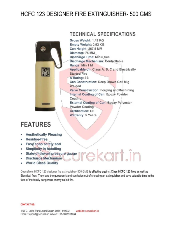
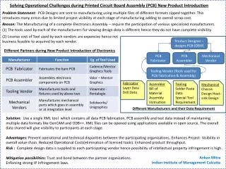
Solving Operational Challenges during Printed Circuit Board Assembly (PCB) New Product Introduction Problem Statement: PCB Designs are sent to manufacturing using multiple files of different formats zipped together. This introduces many errors due to limited project visibility at each stage of manufacturing adding to overall scrap cost. Reason: The Manufacturing of a complete Electronics Assembly – require the participation of various specialized manufacturers. (1) The tools used by each of the manufacturers for viewing design data is different hence they do not have complete visibility. (2) License cost of Tool used by each vendors are expensive hence not business feasible to acquired by each vendor. Product Designer – designs PCB (OEM) Different Partners during New Product Introduction of Electronics PCB Fabricator PCB Assembler Mechanical Vendor Tooling Vendor (Tools used for PCB Fabrication & Assembly) Fabricator Layer Data Drill Data Assembler Bill of Material Assembly Instruction Tooling Solder Paste Data Special Tool Requirement Mechanical Chassis Design Heat-sink Design Different Manufacturers and their Data Requirement Solution: Use a single XML tool which contains all data PCB fabrication, PCB assembly and test data instead of maintaining multiple data formats like GenCAM and ODB++. XML files can be opened using applications available in open source. The overall data shared will give visibility to participants at each stage. Advantages:Prevent operational and technical disparities between the participating organizations. Enhances Project Visibility in overall value chain. Reduced Operational Costs(elimination of licensed tools). Enhanced product throughput. Risk : Complete design data is supplied to each participating vendor hence possibility of intellectual property infringement is high. Mitigation possibilities: Trust and bond between the partner organizations. Enforcing strong IP infringement laws. AnkanMitra Indian Institute of Management Calcutta