Download
1 / 1
10 likes | 203 Vues
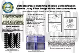
Optoelectronic Multi-Chip Module Demonstration System Using Fiber Image Guide Interconnections Jason D. Bakos, Donald M. Chiarulli, Steven P. Levitan, University of Pittsburgh. Switch Chip Architecture

E N D
Optoelectronic Multi-Chip Module Demonstration System Using Fiber Image Guide Interconnections Jason D. Bakos, Donald M. Chiarulli, Steven P. Levitan, University of Pittsburgh • Switch Chip Architecture • Each switch chip is a full custom Peregrine Semiconductor .5u UTSi silicon-on-sapphire ASIC. Die dimensions are 4mmx6mm. The die is logically divided in half. The optoelectronic side of the die contains: • 64x64 array of modulators and area pads for the flip-chip bonding of a 64x64 MSM GaAs photodetector array (250u pitch) • 64x64 array of VCSEL drivers and area pads for the flip-chip bonding of a 64x64 GaAs VCSEL array (250u pitch) • The other side of the chip contains the logic, configuration cache memory, and configuration mapping memory. • Wire bond pads line three sides of die for electrical I/O. Switch configuration is performed electrically. • The chip is currently in fabrication. We present a demonstration prototype of an optoelectronic 3-chip OE-MCM module that implements a 64 channel non-blocking fiber optic crossbar switch. Each OE-chip implements 64 channels of optical input and output that is guided within the MCM by a optic built from two segments of image guide. Crossbar Architecture The 64x64 crossbar is built using three switch chips. Each switch chip is identical, and each implements eight independent 8x8 crossbar switches. These chips are interconnected to form a full 64x64 crossbar switch. Figure 4: Packaging Architecture Wireframe view of the package internals. Figure 3: Packaging Architecture Arrows indicate the fiber direction. Fiber Image Guide Packaging Technology At the core of the MCM architecture is an optical element built by bonding together two rigid segments of imaging fiber guide. These image guides are produced by Schott Fiber Optics and consist of a dense array of small core fibers arranged in a lattice. Fiber diameters typically range from 5 to 20 microns, yielding core densities of two thousand to fifteen thousand cores per square millimeter. Thus, an array of optical channels imaged on one surface is correspondingly imaged on the opposite surface. It is important to keep in mind that this is an imaging operation. Each optical channel is spatially over-sampled by multiple fiber cores. This is not a core-per-channel arrangement such as you have in a fiber ribbon cable. Switching I/O originates from the fiber cable shown. Figure 1: Crossbar Switch Architecture Each column of 8x8 switches represents one switch chip. Figure 2: Switch Chip Layout The optoelectronic (analog) half of the chip is depicted as the lower half here.