Download
1 / 2
20 likes | 37 Vues
Where automated optical inspection can inspect PCBs thoroughly, automated X-ray inspection can also detect faults in PCBs that have no visible joints. This provides for in-depth analysis of errors that can then be eliminated.

E N D
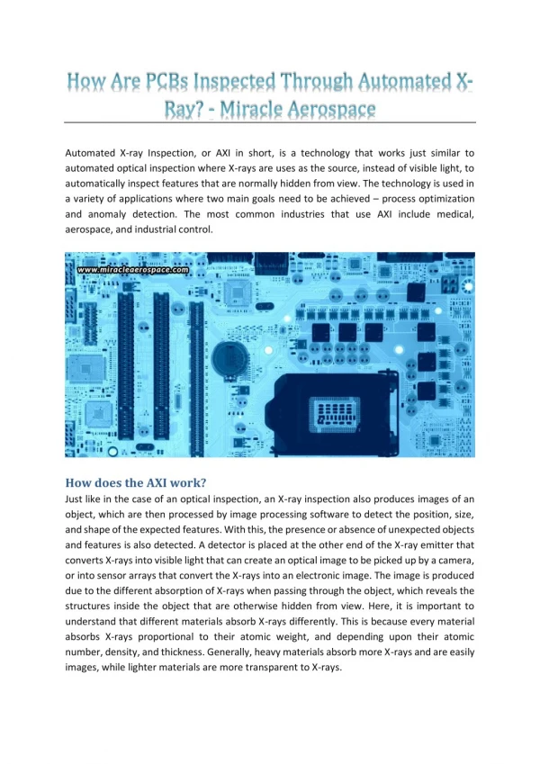
Automated X-ray Inspection, or AXI in short, is a technology that works just similar to automated optical inspection where X-rays are uses as the source, instead of visible light, to automatically inspect features that are normally hidden from view. The technology is used in a variety of applications where two main goals need to be achieved – process optimization and anomaly detection. The most common industries that use AXI include medical, aerospace, and industrial control. How does the AXI work? Just like in the case of an optical inspection, an X-ray inspection also produces images of an object, which are then processed by image processing software to detect the position, size, and shape of the expected features. With this, the presence or absence of unexpected objects and features is also detected. A detector is placed at the other end of the X-ray emitter that converts X-rays into visible light that can create an optical image to be picked up by a camera, or into sensor arrays that convert the X-rays into an electronic image. The image is produced due to the different absorption of X-rays when passing through the object, which reveals the structures inside the object that are otherwise hidden from view. Here, it is important to understand that different materials absorb X-rays differently. This is because every material absorbs X-rays proportional to their atomic weight, and depending upon their atomic number, density, and thickness. Generally, heavy materials absorb more X-rays and are easily images, while lighter materials are more transparent to X-rays.
How is a PCB inspected through AXI? In this blog, we will understand how AXI has been used widely and popularly to inspect a PCB assembly from India. Traditionally, automated optical inspection has been used to inspect PCBs. But this was because earlier PCBs had visible joints. However, many PCBs being produced today don’t have visible solder connections. This has given rise to the need for greater number of interconnections to integrated packages, thus increasing complexity. This is why AXI is now being popularly used as it can not only check the solder joints under components, but can also reveal many defects in the solder joints that may not be visible with optical inspection equipment. Another added benefit with this kind of inspection is that both 2D and 3D technologies are available that brings significant improvements in performance! AXI technologies are able to monitor a variety of aspects of a PCB assembly production. They are not only able to see through the components, but are also able to provide an internal view of solder joints, which helps to detect voids with the joints that may otherwise look perfectly alright. This means that AXI systems can provide additional information over what can be provided by purely optical systems to ensure that solder joints are being made to the required standard by minimizing the defects, thus improving the quality and performance. In addition, the entire production process that follows can be altered to reduce fault levels on the boards. In this way, the highest standards are maintained to bring up optimized and processed new boards in the future. To have the best quality 100% tested PCB for your application, you can get in touch with Miracle Aerospace. Here, you will be provided with PCBs that are manufactured not only with the best resources and a dedicated quality assurance process, but that are also tested completely through both automated and semi-automated systems to provide you with the finest quality error-free PCB assembly from India.