Cache Performance
Cache Performance. Explain the relationship between miss rate and block size in a cache. Construct a flowchart explaining how a cache miss is handled. Compare and contrast write through and write back caching schemes. Define the term write buffer.

Cache Performance
E N D
Presentation Transcript
Cache Performance Explain the relationship between miss rate and block size in a cache. Construct a flowchart explaining how a cache miss is handled. Compare and contrast write through and write back caching schemes. Define the term write buffer. Perform cache related calculations to analyze the impact of having a cache on a computer system.
Consider the lw instruction that loads a word from memory to a register: 23 0x1001004F 0x1001004E 0x1001004D 0x1001004C 0x1001004B 0x1001004A 0x10010049 lw $t0, ($t1) # $t1=0x10010048After loading, $t0 will containthe value 0x2e0267ce. A direct load from main memory would consume many CPU cycles, resulting in a long stall of every lw instruction. 40 01 20 ce Word 67 02 0x10010048 0x10010047 0x10010046 0x10010045 0x10010044 2e 78 63 74 69 CS-280 Dr. Mark L. Hornick
Ex: Direct Address cache, block size of 16B, #blocks=256 (4KB total)lw $t0, ($t1) # t1=0x1001 0048 (4-byte address)The Cache Index is computed from Memory Block Address 0x1001004. The cacheblock at that index is initially empty (Valid bit=0), resulting in a miss. The cache manager loads a block of 16 bytes into cache index 04, from main memory addresses 0x10010040 – 0x1001004F. This initial load from main to cache memory consumes many CPU cycles (~100), resulting in a long stall of this particular lwinstruction. Cache Index = (Memory Block Address) mod (#Blocks in Cache) CS2710 Computer Organization
Once the cache block is loaded, the 4 bytes at address 0x10010048 are loaded into t1.lw $t0, ($t1) # t1=0x1001 0048, t0=0x2e02676e The Valid Bit for the block is set to 1 and the Tag Bits are set to 0x10010. Note that the original address of the memory location of the data can be reconstructed from the Tag Bits (10010) + Cache Index (04) + Byte Offset within the Block (8) CS2710 Computer Organization
Suppose the next instruction attempts to load the subsequent word into t0lw $t0, ($t1) # t1=0x1001 0048, t0=0x2e02676e lw $t0, 4($t1) # load next word from 0x1001 004cThe Cache Index is (again) computed from Memory Block Address 0x1001004. The cacheblock at that index is valid (Valid bit=1), and the tags match, resulting this time in a hit. This subsequent load from cache memory consumes only 1 CPU cycle, avoiding a stall of the lw instruction. CS2710 Computer Organization
The 3rd instruction loads a word from a different location in memorylw $t0, ($t1) # t1=0x1001 0048, t0=0x2e02676e lw $t0, 4($t1) # load next word from 0x1001 004clw $t0, ($sp) # sp=0x7FFF EFFC, t0=0x1928ef3cThe Cache Index is computed from Memory Block Address 0x7FFFEFF. The cacheblock at that index is initially empty (Valid bit=0), resulting in another miss. The cache manager loads a block of 16 bytes into cache index FF, from main memory addresses 0x7FFFEFF0 – 0x7FFFEFFF. Then the word at 0x7FFFEFFC is loaded into $t0. CS2710 Computer Organization
The 4th instruction loads a word …lw $t0, ($t1) # t1=0x1001 0048, t0=0x2e02676e lw $t0, 4($t1) # load next word from 0x1001 004clw $t0, ($sp) # sp=0x7FFF EFFC, t0=0x1928ef3clw $t0, ($t3) # t3=0x2537 1044 The Cache Index is computed from Memory Block Address 0x2537104. The cacheblock at that index is currently valid (Valid bit=1), but the tags don’t match, resulting in a miss. The cache manager reloads a block of 16 bytes into cache index 04, from main memory addresses 0x2537140 – 0x243714F. The value 0xaabbccdd is loaded into $t0. CS2710 Computer Organization
Discussion • An engineer is designing a computer system and is designing a system with either 64KB of cache or 256KB of cache. Which will perform better? • Another engineer is designing a system with 16KB of cache, and is trying to decide whether to use a block size of 16 or 64. Which will perform better? CS2710 Computer Organization
Experimental Results What does this tell us? Increasing total cache size decreases cache misses. Increasing block size decreases miss rate to a point, at which point it starts going up again. CS2710 Computer Organization
Block size considerations • Larger blocks should reduce miss rate • Due to spatial locality • But in a fixed-sized cache • Larger blocks fewer of them • More competition increased miss rate • Larger blocks pollution • Larger miss penalty • Can override benefit of reduced miss rate • Early restart and critical-word-first can help • Larger blocks exploit spatial locality to lower miss rates. • But miss rates increase when the block size becomes a significant portion of the cache size • Larger miss penalty: the larger the block, the longer it takes to load it CS2710 Computer Organization
Handling Misses CS2710 Computer Organization
Suppose the next instruction attempts to write the subsequent word to t1lw $t0, ($t1) # t1=0x1001 0048, t0=0x2e02676e sw $t0, 4($t1) # now store $t0 to 0x1001 004cThe Cache Index is computed from Memory Block Address 0x1001004. The cacheblock at that index is valid (Valid bit=1), and the tags match, resulting in a hit. This subsequent store to cache memory changes the contents of cache, but the main data memory is still (at this point) unchanged and out of sync with the cache. The change to the cache is noted by setting the Dirty Bit to 1. CS2710 Computer Organization
Another instruction loads a word …lw $t0, ($t1) # t1=0x1001 0048, t0=0x2e02676e sw $t0, 4($t1) # now store $t0 to 0x1001 004c lw $t0, ($t3) # t3=0x2537 1044 The Cache Index is computed from Memory Block Address 0x2537104. The cacheblock at that index is currently valid (Valid bit=1), but the tags don’t match, resulting in a miss. The Dirty Bit is also set, indicating that the cache has to be written to main memory before the reload can take place. This results in a double-length stall: first the changed cache has to be written to memory, then the new block needs to be loaded. CS2710 Computer Organization
Approaches to Writing Data to memory But cache and memory would be inconsistent But writes will take longer Buffers data writes. Only causes a stall if the buffer is full • Write through • Update cache plus block in main memory • A separate Write Buffer is used CS2710 Computer Organization
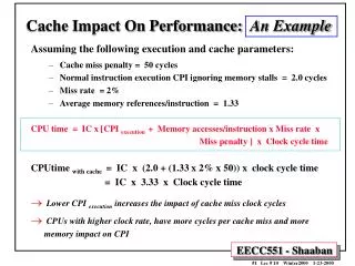
Cache Performance Two different configurations for a cache system are being developed. In both cases, the miss penalty is 100 clock cycles, and the processor has an average CPI of 2 if no memory stalls occur. • The first cache system has a miss rate of 4% in the data cache. • The second system has a miss rate of 2% in the data cache. • 36% of instructions are loads and stores. Determine the performance relationship between processor A and processor B. CS2710 Computer Organization
Problem solution CPIA / CPIB=3.44/2.72=1.26 Processor A is 26% slower than Processor B CS2710 Computer Organization
Average Memory Access Time • Average Memory Access Time (AMAT) • The average of the time (per instruction) it takes to access memory considering both hits and misses. CS2710 Computer Organization
AMAT Problem • Solve the following: • A processor has a 1ns/inst clock cycle time, a miss penalty of 50 clock cycles, a miss rate of 0.1 misses per instruction, and a cache access time of 1 clock cycle. • Determine the average memory access time per instruction. CS2710 Computer Organization
Solution CS2710 Computer Organization

