Enhancing Cache Memory Performance: Optimization Strategies and Techniques
This article explores essential strategies to enhance cache memory performance by analyzing average memory access time components: hit time, miss rate, and miss penalty. It delves into techniques to reduce miss rates through larger caches, minimize miss penalties with L2 caches, and optimize hit time without affecting clock speed. It covers types of cache misses—compulsory, capacity, and conflict—and discusses advanced topics such as sub-block placement, prefetching techniques, and memory architecture design. Effective code restructuring and selective data caching further improve overall system performance.

Enhancing Cache Memory Performance: Optimization Strategies and Techniques
E N D
Presentation Transcript
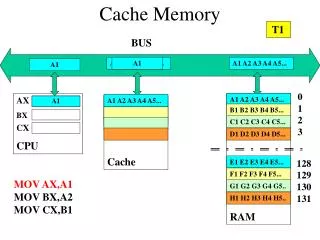
Average memory access time = Hit time + Miss rate x Miss penalty To improve performance: • reduce the miss rate (e.g., larger cache) • reduce the miss penalty (e.g., L2 cache) • reduce the hit time The simplest design strategy is to design the largest primary cache without slowing down the clock or adding pipeline stages Design the largest primary cache without slowing down the clock Or adding pipeline stages.
• Compulsory: first-reference to a block a.k.a. cold start misses -misses that would occur even with infinite cache • Capacity: cache is too small to hold all data needed by the program -misses that would occur even under perfect placement & replacement policy • Conflict: misses that occur because of collisions due to block-placement strategy -misses that would not occur with full associativity
Tags are too large, i.e., too much overhead – Simple solution: Larger blocks, but miss penalty could be large. • Sub-block placement – A valid bit added to units smaller than the full block, called sub-locks – Only read a sub-lock on a miss – If a tag matches, is the word in the cache? Main reason for sub-block placement is to reduce tag overhead.
-Writes take two cycles in memory stage, one cycle for tag check plus one cycle for data write if hit -Design data RAM that can perform read and write in one cycle, restore old value after tag miss -Hold write data for store in single buffer ahead of cache, write cache data during next store’s tag check -Need to bypass from write buffer if read matches write buffer tag
Speculate on future instruction and data accesses and fetch them into cache(s) – Instruction accesses easier to predict than data accesses • Varieties of prefetching – Hardware prefetching – Software prefetching – Mixed schemes • What types of misses does prefetching affect?
• Usefulness – should produce hits • Timeliness – not late and not too early • Cache and bandwidth pollution
• Instruction prefetch in Alpha AXP 21064 – Fetch two blocks on a miss; the requested block and the next consecutive block – Requested block placed in cache, and next block in instruction stream buffer
Prefetch-on-miss accessing contiguous blocks Tagged prefetch accessing contiguous blocks
• What property do we require of the cache for prefetching to work ?
Restructuring code affects the data block access sequence – Group data accesses together to improve spatial locality – Re-order data accesses to improve temporal locality • Prevent data from entering the cache – Useful for variables that are only accessed once • Kill data that will never be used – Streaming data exploits spatial locality but not temporal locality
• Upon a cache miss – 4 clocks to send the address – 24 clocks for the access time per word – 4 clocks to send a word of data • Latency worsens with increasing block size Need 128 or 116 clocks, 128 for a dumb memory.
Banks are often 1 word wide • Send an address to all the banks • How long to get 4 words back? 4 + 24 + 4* 4 clocks = 44 clocks from interleaved memory.
Send an address to all the banks • How long to get 4 words back? 4 + 24 + 4 = 32 clocks from main memory for 4 words.
Consider a 128-bank memory in the NEC SX/3 where each bank can service independent requests