CACHE MEMORY
CACHE MEMORY. Characteristic of Memory System. Location Processor - Requires its own local memory. Internal memory - Is often equated with main memory.

CACHE MEMORY
E N D
Presentation Transcript
Characteristic of Memory System • Location • Processor - Requires its own local memory. • Internal memory - Is often equated with main memory. • External memory - Consists of peripheral storage device such as disk and tape , that are accessible to the processor via I/O controllers • Capacity • For internal memory, this is typically expressed in terms of bytes (1 Byte = 8 Bits)or words. Common word lengths are 8, 16, and 32 bits. • For external memory, , this is typically expressed in terms of bytes.
Unit of Transfer • For internal memory, the unit of transfer is equal to the number of data lines and out of the memory module. This maybe equal to the word length, but is often larger such as 64, 128, or 256. Three related concept: • Word: The “ natural” unit of organization of word. • Addressable Unit: In some systems, the addressable unit is the word • Unit of Transfer: For main memory, this is the number of bits read out of or written into memory at a time. • For external memory, data are often transferred in much larger units than a word, and these are referred to as blocks.
Access Method • Sequential Access- Memory is organized into units o data, called records. • Direct Access- As with sequential access, direct access involves a shared read-write mechanism. • Random Access- Main memory and some cache system are random access. • Associative- This is a random –access type of memory that enables one to make a comparison of desired bit locations within a word for a specified match, and to do this for all words simultaneously.
Performance • Three performance parameters • Access time (latency)- For random access memory, this is the time it takes to perform a read or write operation, that is, the time from the instant that an address is presented to the memory to the instant that data have been stored or made available for use. For non-random access memory, access time is the time it takes to a position the read-write mechanism at the desired location. • Memory cycle time- this is primarily applied to random access memory and consists of the access time plus any additional time required before a second access can commence.
Transfer rate- This is the rate at which data can be transferred into or out of a memory unit. For random access memory , it is equal to 1/(cycle time). For non-random access memory, the ff. relationship holds: T = T + N/R where T = Average time to read or write N bits T = Average access time N = Number of bits R = Transfer rate, in bits per second(bps)
Physical Type • The most common today are : • Semiconductor memory • Magnetic surface memory • Used for disk and tape and optical • Magneto-optical • Physical Characteristics • In a volatile memory, information decays naturally or is lost when electrical power is switches off. In nonvolatile memory, information once record remains without deterioration until deliberately changed; no electrical power is needed to retain information. Magnetic surface memories are nonvolatile. Semi conductor memory may be either volatile or nonvolatile. Nonerasable memory cannot be altered, except by destroying the storage unit. It is called as Random access memory(ROM).
Organization • By organization is meant the physical arrangement of bits to form words. The obvious arrangement is not always used, as will be explained presently.
Memory Hierarchy • The design constraint on a computer’s memory can be assumed up by three question’s: • How much? :The question of how much is somewhat open ended. • How fast?:The question of how fast is, in a sense, easier to answer . • How expensive?: The final question must also considered. • Three key characteristic of memory: • Cost • Capacity • Access time
At any given time, a variety of technologies are used to implement memory systems. Across this spectrum of technologies, the following relationships hold: • Faster access time, greater cost per bit • Greater capacity, smaller cost per bit • Greater capacity, slower access to time The dilemma facing the designer is clear. The way of this dilemma is not to rely on a single memory component or technology, but to employ a memory hierarchy. A typical hierarchyis illustrated in a figure4.1
a. Decreasing cost per bit b. Increasing capacity c. Increasing access time d. Decreasing frequency of access of the memory by the processor Thus smaller, more expensive , faster memories are supplemented by larger, cheaper, slower memories. The key to success of this organization is item (d): Decreasing frequency of access.
T₁ + T₂ T₂ Average access time T₁ 0 Fraction of accesses involving only level 1 (hit ratio) Figure 4.2 Performance of a Two-Simple Level Memory
The use of two levels of memory to reduce average access time works in principle, but only if condition (a)through (d)apply. By employing a variety of technologies, a spectrum of memory systems exists that satisfies conditions (a) through (c) fortunately, condition (d) is also generally valid. The basis for the validity of condition (d) is a principle known as locality of reference [DENN68]. This principle can be applied across more than two levels of memory, as suggested by the hierarchy shown in figure 4.1. the fastest, smallest, and most expensive type of memory consists of the register internal to the processor.
The three forms of memory just described are • typically, • volatile • employ semiconductor technology. • Data -are stored more permanently on external mass storage device of magnetic disk, tape, and optical storage. • External nonvolatile memory – is also referred to as secondary or auxiliary memory. Other form of memory may be included in the hierarchy. • Expanded Storage- large IBM mainframes include a form of internal memory. This uses semiconductor technology that is slower and less expensive than that of main memory. This memory does not fit into the hierarchy but is a side branch.
Data can be moved between main memory and expanded storage but not between expanded storage and external memory. • Other forms of secondary memory include optical and magneto-optical disk. Finally additional level can be effectively added to the hierarchy in software. A portion of main memory can be used as a buffer to hold data temporarily that is to be reach out to disk. Such a technique; sometimes referred to as improves performance in to ways; • Disk writes are clustered. Instead of many small transfers of data, we have a few large transfers of data. This improves disk performance and minimizes processor involvement.
Some data destined for write-out may be referenced by a program before the next dump to disk. In that case, the data retrieved rapidly from the software cache rather than slowly from the disk. Cache Memory Principles • Cache memory is intended to give memory speed approaching of the fastest memory available, and at the same time provide a larger memory size at the price of less expensive types of semiconductors memories.
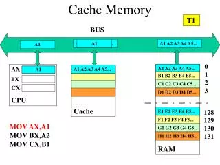
Block Transfer Word Transfer MAIN MEMORY CPU CACHE Figure 4.3 Cache and Main Memory
Memory Address Line Number Tag 0 1 2 C-1 Block (K Words) Block Length (K Words) Block (a) Cache 2n - 1 Word Length Figure 4.4 Cache/Main Memory Structure (b) Main Memory
START Receive Address RA from CPU Is block containing RA in Cache? Access main memory for block containing RA Allocate cache line for main memory block Fetch RA word and deliver to CPU Load main memory block into cache line Deliver RA word to CPU DONE Figure 4.5 Cache read Operation
Address Address Buffer cache Processor Control Control System Bus Data Buffer Data Fig. 4.6 Typical Cache Organization
Elements of Cache Design • High Performance Computing(HPC)-Deals with supercomputers and supercomputers software, especially for scientific applications that involve large amount of data, vector and matrix computation, and the use of parallel algorithms. • Cache design for HPC is quite different for other hardware platforms and applications.
Cache Size The larger the cache , the larger the number of gates involve in addressing the cache. The result is that larger cache tend to be slightly lower than small ones---even when built with the same integrated circuit technology and put in the same place on chip and circuit board. • Mapping Function • Because there are fewer cache lines than main memory blocks, an algorithm is needed for mapping main memory blocks into cache lines. Further a means is needed for determining which main memory block currently occupies a cache line. The choice of mapping function dictates how the cache is organized.
Direct Mapping- The simplest technique, known as direct mapping , maps each block of main memory into only one possible cache line. The mapping is expressed by: i = j modulo m where I=cache line number j=main memory block number m=number of lines in the cache The mapping function is easily implemented using the address. For purposes of cache access, each main memory address can be viewed as consisting of three fields. The list significant w bits identify a unique word or byte within a block of main memory; in most contemporary machines, the address is at the byte level. The remaining s bits specify one of the 2 raise s blocks of main memory. The cache logic interprets these s bits as a tag of s -- r bits(most significant portion) and a line field of r bits.
This later fields identifies one of the m = 2 raise to r lines of the cache. To summarize: • Address length= (s+ u) bits • Number of addressable units = 2 raise to (s+w) words or bytes • Block size = line size = 2 raise to w words or bytes • Number of block line in main memory = 2 raise to (s+w) over 2 raise to w = 2 raise to s • Number of lines in cache = m = 2 raise to r • Size of tag = (s-- r) bits
The effect of this mapping is that blocks of main memory are assigned to lines of the cache as follows: • Thus, the use of a portion of the address as a line number provides a unique mapping of each block of main memory into the cache. When block is actually read into its assigned line, it is necessary to tag the data to distinguish it from other blocks that can fit into that time. The most significant s—r bit serve this purpose.
Line + Tag word Data 0000 0004 FFF8 FFFC 13579246 Line number Tag Data 00 16 16 FF 16 13579246 11235813 FEDCBA98 11223344 12345678 0000 0001 0CE7 3FFE 3FFF 0000 0004 339C FFFC 77777777 11235813 FEDCBA98 12345678 8 bits 32bits 16-Kline cache 0000 0004 FFF8 FFFC Tag Line word Main memory address= Figure 4.8 Direct Mapping Example 11223344 24682468 32 Bits 16-Mbits main memory
The direct mapping technique is simple and inexpensive to implement. Its main disadvantage is that there is a fixed cache location for any give block. Thus, if a program happens to reference words repeatedly from two different blocks that map into the same line, then the blocks will continually swapped in the cache, and the hit ratio will be low(a phenomenon knows as thrashing). • Associative Mapping • Associative mapping overcome the disadvantage of direct mapping by permitting each main memory blocks to be loaded into any line of the cache. In this case, the case control logic interprets a memory address simply as a tag and a word field. The tag field uniquely identifies a block of main memory. To determine whether a block is in the cache, the case control logic must simultaneously examine every line’s tag for a match.
Note: no field in the address corresponds to line number, so that the number of lines in the case is not determined by the address format. To summarized: • Address length = (s + w) bits • Number of addressable units = words or bytes • Block size= line size= words or bytes • Number of blocks in main memory= = • Number of lines in cache= undetermined • Size of tag=sbits
cache Tag Data Memory address s w w X x (Hit in cache) s (Miss in cache)
13579246 Associative Mapping line number address 0000 000000 0001 000004 163398 3FFD 16339C 3FFE 1633AC 3FFF FFFFF4 11223344 16-kline cache FFFFFC Tag word main memory= FEDCBA98 22 bits 32 bits 33333333 11223344 24682468
Set associative Mapping • Set associative mapping is compromise that exhibits the strengths of both the direct and associative approaches while reducing their disadvantages. In this case, the cache divided into v sets, each of which consists of k lines. The relationship are: m=v x k i= j modulo v Where i=cache set number j=main memory block number m=number of lines in the cache This is referred to ask k-way set associative mapping. With associative mapping block can be mapped into any lines of seti. In this case, the cache control logic interprets a memory address simply as three fields: tag, set and word. The d set bits specify one of v= sets. The s bits of tag and set field specify one of the blocks of main memory.
With k-wayset associative mapping, the tag in a memory address is much smaller and is only compared to the k tags within a single set. To summarized: • Address length = (s + w) bits • Number of addressable units = words or bytes • Block size = line size= words or bytes • Number of blocks in main memory= = • Number of line in set = k • Number of sets = v = • Number of lines in cache = k v = k x • Sixe of tag = (s-d) bits
s + w Main memory Tag Data K-Way Set Associative Mapping S-d d w Set0 …. s-d S + w X X set1 (Hit in cache) (miss in cache)
Two-ways Associative Mapping Set + word 0000 0004 0 7FF8 7FFC Set Number 0000 0004 000 001 12C OCE7 339C 7FFC 1FFE 1FFF 9 bits 32 bits 9 bits 32 bits 0000 0004 16-kline cache 1FF 7FF8 7FFC Tag Set Word 32 bits Main memory Address = 16-Mbyte main memory
In the extreme case of v=m, k=1, the set associative technique reduces to associative mapping. The use of two lines per set(v=m/2, k=2) is the most common set associative organization. If significantly improves the hit ratio over direct mapping. Four-way set associative (v=m/4, k=4) makes a modest additional improvement for a relatively small additional cost[MAYB84,HILL89]. Further increases in number of lines per set have little effect.
Replacement Algorithm • To achieve a high speed , such an algorithm must be implemented in a hardware. A number of algorithm have been tried: we mention four of the most common. Probably the most effective is least recently use(LRU); Replace that block in the set that has been in the cache longest with no reference to it. For two way set associative, this is easily implemented. Each lines includes a USE bit. When a line is referenced, its USE bit is set to 1 and the USE bit of the other line in that set is set to 0. when block is to be read into the set, the line whose USE bit is 0 is use because we are assuming that more recently use memory locations are likely to be referenced, LRU should give the best hit ratio.
Another possibility is first-in –first-out (FIFO); replace that block in he set that has been in the cache longest. FIFO is easily implemented as around-robin or circular buffer technique. Still another accessibility's list frequently used( LFU); replaced that block ion the set that has experienced the fewest references. LFU implemented by associating a counter with each line. A technique not base on usage is to pick a line at random from among the candidate lines.
Write Policy • When a block is resident in the cache to be replaced, there are two cases to consider: • If the old block in the cache has not been altered, then it maybe over written with a new block without first writing out the old block. • If at least one write operation has been performed on a word in that line of the cache, then main memory must be updated by writing the line of each out to the block of memory before bringing in the new block. • A more complex problem occur when multiple processor are attached to the same bus and each processor has its own local cache. Then, if the word is altered in one cache. It could conceivably invalidate a word and other cache. • The simplest technique is called write through.
Possible approaches to cache coherency include: • Bus watching with write through. If another master writes to a location in shared memory that also resides in the cache memory, the cache controllers invalidates the cache entry. • Hardware transparency. Additional hardware issued to ensure that all updates to main memory via cache are reflected in all caches. Thus, if one processors modifies word in its cache, this update is written to main memory. • Non-cacheable memory . In such a system, all access to shared memory are cache misses , because the cache memory is never copied into the cache.
Line Size • When a block of data is retrieved and placed in the cache, not only the desired word that also some number of adjustment words are retrieved. • The hit ratio will begin to decrease, however, as block becomes even bigger and probability of reusing the information that has to be replaced. Two specific effects come into play: • Larger blocks reduce the number of block that fit into a cache. Because each block fetch over write older cache contents, a small number of blocks result in data being overwritten shortly after they are fetched. • As a block becomes larger, each additional word is farther from the requested word, therefore, less likely to be needed in the near future.
Number of Cache Two aspects of this design issue concern the number of level of cache and the use of unified versus split caches. • Multilevel caches. Compared with a cache reachable via an external bus, the on-chip cache reduces the processors external bus activity and therefore speeds up execution times and increases overall system performance. Because of the short data paths internal to the processor, compare with bus lengths, on-chip cache accesses will complete appreciably faster than would even zero-wait state bus cycle.
Unified versus Split Cache • When the on-chip cache first made an appearance, many of the design consisted of a single cache used to store references to both data and instruction. • Describe these advantages, the trend is toward split cache particularly for superscalar machine such as the Pentium and power PC, which emphasize parallel instruction execution and the prefetching of predicted future instruction. Suppose now that we have unified instruction data cache. When the execution unit performs a memory access to load and store data, the request is submitted to the unified cache.
Pentium 4 and Power PC Cache Organization • The evolution of cache organization is seen clearly in the evaluation of Intel microprocessor. The 80386 does not include on-chip cache. The 80486 includes a single on-chip cache of 8k bytes using a line size of 16 bytes in a four way set associative organization.
All of the Pentium include two on-chip L1 caches, one for data and one for instruction. For Pentium 4, the L1 data cache is 8k bytes, using a line size of 64 bytes and a four-way set associative organization. • The Pentium 4 instruction cache described subsequently. The Pentium 2 also include an L2 cache that feeds both of the L1 caches. The L2 cache is eight-way set associative with the size of 256 kb and a line size of 128 bytes. An L3 cache was added for the Pentium 3 and became on-chip with high-end versions of Pentium 4.
The processor core consists of four major components: • Fetch/decode unit : Fetches program instructions in order from the L2 cache , decodes these into a series of micro-operations , and stores the result in the L1 instruction cache. • Out-of-order execution logic : Schedules execution of the micro-operations subject to data dependencies and resource availability; thus , micro-operations may be scheduled for execution in a different order than they were fetched from the instruction stream. As time permits, this unit schedules speculative execution of micro-operations that may be required in the future.
Execution units : These units executes micro-operations , fetching the required data from the L1 data cache and temporarily storing results in registers. • Memory subsystem: This unit includes the L2 and L3 caches and the system bus, which is used to access main memory when the L1 and L2 caches have a cache miss, and to access the system I/O resources. • The Pentium 4 instruction cache sits between the instruction decode logic and the execution core.
The Pentium process decodes, or translates. Pentium machine instruction into simple, fixed-length micro-operations enables the use of superscalar pipelining and scheduling techniques that enhance performance. However, the Pentium machine instruction are cumbersome to decode; they have a variable number of bytes and many different options. It turns out that performance is enhanced if this decoding is done independently of the scheduling and pipelining logic. • The data cache employs a write-back policy: data are written to memory only when they are removed from the cache and there has been an update. The Pentium 4 processor can be dynamically configured to support write-through caching.