Chapter 3 Basics Semiconductor Devices and Processing
Chapter 3 Basics Semiconductor Devices and Processing. Hong Xiao, Ph. D. www2.austin.cc.tx.us/HongXiao/Book.htm. Objectives. Identify at least two semiconductor materials from the periodic table of elements List n-type and p-type dopants Describe a diode and a MOS transistor

Chapter 3 Basics Semiconductor Devices and Processing
E N D
Presentation Transcript
Chapter 3Basics Semiconductor Devices and Processing Hong Xiao, Ph. D. www2.austin.cc.tx.us/HongXiao/Book.htm www2.austin.cc.tx.us/HongXiao/Book.htm
Objectives • Identify at least two semiconductor materials from the periodic table of elements • List n-type and p-type dopants • Describe a diode and a MOS transistor • List three kinds of chips made in the semiconductor industry • List at least four basic processes required for a chip manufacturing www2.austin.cc.tx.us/HongXiao/Book.htm
Topics • What is semiconductor • Basic semiconductor devices • Basics of IC processing www2.austin.cc.tx.us/HongXiao/Book.htm
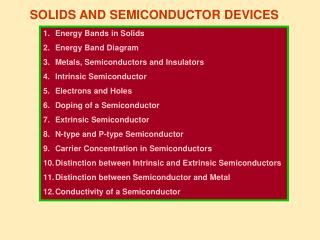
What is Semiconductor • Conductivity between conductor and insulator • Conductivity can be controlled by dopant • Silicon and germanium • Compound semiconductors • SiGe, SiC • GaAs, InP, etc. www2.austin.cc.tx.us/HongXiao/Book.htm
Periodic Table of the Elements www2.austin.cc.tx.us/HongXiao/Book.htm
Semiconductor Substrate and Dopants Substrate P-type Dopant N-type Dopants www2.austin.cc.tx.us/HongXiao/Book.htm
Orbital and Energy Band Structure of an Atom Valence shells Conducting band, Ec Nuclei Band gap, Eg Valence band, Ev www2.austin.cc.tx.us/HongXiao/Book.htm
Band Gap and Resistivity Eg = 1.1 eV Eg = 8 eV Aluminum 2.7 mWcm Sodium 4.7 mWcm Silicon ~ 1010 mWcm Silicon dioxide > 1020mWcm Conductors Semiconductor Insulator www2.austin.cc.tx.us/HongXiao/Book.htm
Crystal Structure of Single Crystal Silicon www2.austin.cc.tx.us/HongXiao/Book.htm
Why Silicon • Abundant, inexpensive • Thermal stability • Silicon dioxide is a strong dielectric and relatively easy to form • Silicon dioxide can be used as diffusion doping mask www2.austin.cc.tx.us/HongXiao/Book.htm
Si Si Si Extra Si As Si Si Si Si - N-type (Arsenic) Doped Silicon and Its Donor Energy Band Conducting band, Ec Ed ~ 0.05 eV Electron Eg = 1.1 eV Valence band, Ev www2.austin.cc.tx.us/HongXiao/Book.htm
Conducting band, Ec Si Si Si Hole Eg = 1.1 eV Si B Si Ea ~ 0.05 eV Si Si Si - Valence band, Ev Electron P-type (Boron) Doped Silicon and Its Donor Energy Band www2.austin.cc.tx.us/HongXiao/Book.htm
Conducting band, Ec Conducting band, Ec Eg = 1.1 eV Eg = 1.1 eV Electron Electron Conducting band, Ec Valence band, Ev Valence band, Ev Hole Hole Eg = 1.1 eV Electron Ea ~ 0.05 eV Valence band, Ev Hole Illustration of Hole Movement www2.austin.cc.tx.us/HongXiao/Book.htm
Dopant Concentration and Resistivity Resistivity P-type, Boron N-type, Phosphorus Dopant concentration www2.austin.cc.tx.us/HongXiao/Book.htm
Dopant Concentration and Resistivity • Higher dopant concentration, more carriers (electrons or holes) • Higher conductivity, lower resistivity • Electrons move faster than holes • N-type silicon has lower resistivity than p-type silicon at the same dopant concentration www2.austin.cc.tx.us/HongXiao/Book.htm
Basic Devices • Resistor • Capacitor • Diode • Bipolar Transistor • MOS Transistor www2.austin.cc.tx.us/HongXiao/Book.htm
Resistor r h l w r: Resistivity www2.austin.cc.tx.us/HongXiao/Book.htm
Resistor • Resistors are made by doped silicon or polysilicon on an IC chip • Resistance is determined by length, line width, height, and dopant concentration www2.austin.cc.tx.us/HongXiao/Book.htm
Capacitors k l h d k: Dielectric Constant www2.austin.cc.tx.us/HongXiao/Book.htm
Capacitors • Charge storage device • Memory Devices, esp. DRAM • Challenge: reduce capacitor size while keeping the capacitance • High-k dielectric materials www2.austin.cc.tx.us/HongXiao/Book.htm
Capacitors Dielectric Layer Dielectric Layer Poly 2 Poly Si Si Poly Si Oxide Si Poly 1 Heavily Doped Si Parallel plate Stacked Deep Trench www2.austin.cc.tx.us/HongXiao/Book.htm
Metal Interconnection and RC Delay k Dielectric, r Metal, I l d w www2.austin.cc.tx.us/HongXiao/Book.htm
Diode • P-N Junction • Allows electric current go through only when it is positively biased. www2.austin.cc.tx.us/HongXiao/Book.htm
Diode www2.austin.cc.tx.us/HongXiao/Book.htm
Figure 3.14 Transition region - - + + - - + + P N - - + + - - + + - - + + V n V 0 V p www2.austin.cc.tx.us/HongXiao/Book.htm
Intrinsic Potential • For silicon V0 ~ 0.7 V www2.austin.cc.tx.us/HongXiao/Book.htm
I-V Curve of Diode www2.austin.cc.tx.us/HongXiao/Book.htm
Bipolar Transistor • PNP or NPN • Switch • Amplifier • Analog circuit • Fast, high power device www2.austin.cc.tx.us/HongXiao/Book.htm
B E C N P N B E C P N P NPN and PNP Transistors www2.austin.cc.tx.us/HongXiao/Book.htm
NPN Bipolar Transistor Emitter Base Collector Al•Cu•Si SiO2 n n + + p p+ p+ n-epi Electron flow n+ buried layer P-substrate www2.austin.cc.tx.us/HongXiao/Book.htm
Sidewall Base Contact NPN Bipolar Transistor Metal CVD oxide CVD oxide CVD oxide Base Emitter Collector Poly p p n+ Field oxide Field oxide Field oxide n Epi n+ n+ Buried Layer P-substrate www2.austin.cc.tx.us/HongXiao/Book.htm
MOS Transistor • Metal-oxide-semiconductor • Also called MOSFET (MOS Field Effect Transistor) • Simple, symmetric structure • Switch, good for digital, logic circuit • Most commonly used devices in the semiconductor industry www2.austin.cc.tx.us/HongXiao/Book.htm
NMOS DeviceBasic Structure V V G D VG “Metal” Gate VD Ground + + n n p-Si Drain Source www2.austin.cc.tx.us/HongXiao/Book.htm
NMOS Device Positive charges V > V > 0 V > 0 V = 0 Electron flow G T V D G D “Metal” Gate + + + + + + + SiO SiO - - - - - - - 2 2 + + n n + + n n p-Si p-Si Drain Drain Source Source No current Negative charges www2.austin.cc.tx.us/HongXiao/Book.htm
PMOS Device Negative charges V < V < 0 Hole flow V > 0 V = 0 G T V D G D “Metal” Gate - - - - - - - SiO SiO 2 + + + + + + + 2 + + p p + + p p n-Si n-Si Drain Drain Source Source No current Positive charges www2.austin.cc.tx.us/HongXiao/Book.htm
MOSFET www2.austin.cc.tx.us/HongXiao/Book.htm
MOSFET Source, drain, gate Source/drain biased Voltage on gate to turn-on Current flow between source and drain Drinking Fountain Source, drain, gate valve Pressurized source Pressure on gate (button) to turn-on Current flow between source and drain MOSFET and Drinking Fountain www2.austin.cc.tx.us/HongXiao/Book.htm
Basic Circuits • Bipolar • PMOS • NMOS • CMOS • BiCMOS www2.austin.cc.tx.us/HongXiao/Book.htm
Devices with Different Substrates • Bipolar • MOSFET • BiCMOS Dominate IC industry Silicon Germanium • Bipolar: high speed devices • GaAs: up to 20 GHz device • Light emission diode (LED) Compound www2.austin.cc.tx.us/HongXiao/Book.htm
Compound 100% 4% 8% Bipolar 50% 88% MOSFET 1980 1990 2000 Market of Semiconductor Products www2.austin.cc.tx.us/HongXiao/Book.htm
Bipolar IC • Earliest IC chip • 1961, four bipolar transistors, $150.00 • Market share reducing rapidly • Still used for analog systems and power devices • TV, VCR, Cellar phone, etc. www2.austin.cc.tx.us/HongXiao/Book.htm
PMOS • First MOS field effect transistor, 1960 • Used for digital logic devices in the 1960s • Replaced by NMOS after the mid-1970s www2.austin.cc.tx.us/HongXiao/Book.htm
NMOS • Faster than PMOS • Used for digital logic devices in 1970s and 1980s • Electronic watches and hand-hold calculators • Replaced by CMOS after the 1980s www2.austin.cc.tx.us/HongXiao/Book.htm
CMOS • Most commonly used circuit in IC chip since 1980s • Low power consumption • High temperature stability • High noise immunity • Symmetric design www2.austin.cc.tx.us/HongXiao/Book.htm
CMOS Inverter Vdd PMOS V in Vout NMOS Vss www2.austin.cc.tx.us/HongXiao/Book.htm
CMOS IC n+ Source/Drain p+ Source/Drain Gate Oxide Polysilicon STI USG p-Si n-Si Balk Si www2.austin.cc.tx.us/HongXiao/Book.htm
BiCMOS • Combination of CMOS and bipolar circuits • Mainly in 1990s • CMOS as logic circuit • Bipolar for input/output • Faster than CMOS • Higher power consumption • Likely will have problem when power supply voltage dropping below one volt www2.austin.cc.tx.us/HongXiao/Book.htm
IC Chips • Memory • Microprocessor • Application specific IC (ASIC) www2.austin.cc.tx.us/HongXiao/Book.htm
Memory Chips • Devices store data in the form of electric charge • Volatile memory • Dynamic random access memory (DRAM) • S random access memory (SRAM) • Non-volatile memory • Erasable programmable read only memory (EPROM) • FLASH www2.austin.cc.tx.us/HongXiao/Book.htm
DRAM • Major component of computer and other electronic instruments for data storage • Main driving force of IC processing development • One transistor, one capacitor www2.austin.cc.tx.us/HongXiao/Book.htm

