Reconfigurable Processors: Architecture and Compilation Study
300 likes | 393 Vues
Explore the architecture and compilation strategies for reconfigurable processors, focusing on instruction set compilation and register file data bandwidth challenges. Includes motivational examples, ASIP constraints, and proposed compilation flows.

Reconfigurable Processors: Architecture and Compilation Study
E N D
Presentation Transcript
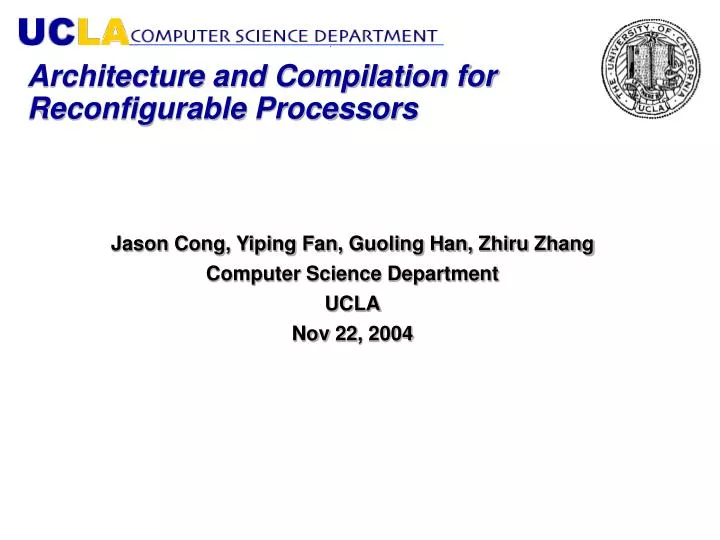
Architecture and Compilation for Reconfigurable Processors Jason Cong, Yiping Fan, Guoling Han, Zhiru Zhang Computer Science Department UCLA Nov 22, 2004
Outline • Motivation • Application-specific instruction set compilation • Register file data bandwidth problem • Architecture extension – shadow registers • Shadow register binding • Conclusions
Reconfigurable Processor Core Bus CPU Reconfigurable Processor Platform • Reconfigurable processor (RP) core + programmable fabric • RP core supports: Basic instruction set + customized instructions • Programmable fabric implements the customized instructions • Either runtime reconfigurable or pre-synthesized • Example: Nios / Nios II from Altera • Stratix version supported by Nios 3.0 system • 5 extended instruction formats • Up to 2048 instructions for each format
a b c 2 5 * * * + + + Motivational Example t1 = a * b; t2 = b * 2;; t3 = c * 5; t4 = t1 + t2; t5 = t2 + t3; t6 = t5 + t4; • t1 = extop1(a, b, 2); • t2 = extop2(b, c, 2, 5); • t3 = t1 + t2; extop2 extop1 *: 2 clock cycles +: 1 clock cycle Extended Instruction Set: Iextop1 expop2 Execution time: 9 clock cycles Execution time: 5 clock cycles Speedup: 1.8
Problem Statement Given: • Application program in CDFG G(V, E) • A processor with basic instruction set I • Pattern constraints: • Number of inputs less than Nin; • 1 output; • Total area no more than A Objective: • Generate a pattern library P • Map G to the extended instruction set IP, so that the total execution time is minimized.
C ASIP constraints Compilation Pattern Generation / CDFG Pattern Selection Pattern Library Application Mapping Mapped CDFG Instruction Implementation / ASIP Synthesis Simulation Implementation Proposed ASIP Compilation Flow • Extended Instruction Candidates Generation • Satisfying I/O constraints • Extended Instruction Selection • Select a subset to maximize the potential speedup while satisfying the resource constraint • Code Generation • Graph covering • Minimize the total execution time
n1 n3 n2 n4 n5 n6 a b c 2 5 * * * + + + Step 1. Pattern Enumeration • Each pattern is a Nin-feasible cone • Cut enumeration is used to enumerate all the Nin-feasible cones [cong et al, FPGA’99] • Basic idea: In topological order, merge the cuts of fan-ins and discards those cuts not Nin-feasible 3-feasible cones: n1: {a, b} n2: {b, 2} n3: {c, 5} n4: {n1, n2}, {n1, b, 2}, {n2, a, b}, {a, b, 2}
a b c 2 5 * * * + + + Step 2. Pattern Selection • Basic idea: simultaneously consider speed up, occurrence frequency and area. • Speedup Tsw(p) = total execution time with basic instructions Thw(p)= length of the critical path of scheduled p Speedup(p) = Tsw(p) / Thw(p) • Occurrence • Some pattern instances may be isomorphic • Graph isomorphism test [ Nauty Package ] • Small subgraphs, isomorphism test is very fast Gain(p) = Speedup(p) Occurrence(p) • Selection under area constraint can be formulated as a 0-1 knapsack problem n3 n2 n1 n4 n5 n6 Pattern *+ Tsw= 3 Thw= 2 Speedup = 1.5
Step 3. Application Mapping • Assume execution on an in-order, single-issue processor • Cover each node in G(V, E) with the extended instruction set to minimize the execution time. • Trivial pattern – software execution time • Nontrivial pattern – hardware execution time • Total execution time = Sum of execution time of instance patterns after application mapping • Theorem: The application mapping problem is equivalent to the library-based minimum-area technology mapping problem.
Simulation Environment • Simplescalar v3.0 • Benchmarks • From Mediabench suite • Machine Configuration • Single issue in-order processor (ARM like) • DL1: 8KB, 4-way, 1 cycle • IL1: 8KB, direct mapped, 1 cycle • Unified L2: 256KB, 4-way, 8 cycle • Functional units: 2 IntAdd, 1 IntMult, 1 FPAdd, 1 FPMult • Reconfigurable units • critical path latency of the collapsed instructions
Pattern Distribution Most of the patterns have less than 7 nodes inside
Outline • Motivation • Application-specific instruction set compilation • Register file data bandwidth problem • Architecture extension – shadow registers • Shadow register binding • Conclusions
Register File Bandwidth Problem • Most of the speedup comes from clusters with more than two inputs • 2-port register file in embedded processors • Need extra cycles to transfer data for extended instructions with more than 2 inputs • Speedup drop due to communication overhead
Speedup Drop with Different Input Constraints • Move operation takes one cycle • 46% speedup drop on average
Outline • Motivation • Application-specific instruction set compilation • Register file data bandwidth problem • Architecture extension – shadow registers • Shadow register binding • Conclusions
Architecture Extensions • Existing Solutions • Dedicated Data Link • Avoid potential resource contention through bus • Need extra cycles for communication • Employed in Microblaze from Xilinx • Multiport Register File • Low utilization when executing basic instructions • Area and power grows cubically • Register File Replication • Predetermined one-to-one correspondence • Resource waste in terms of area and power • Limit compiler optimization
Our Approach – Shadow Registers • Core registers are augmented by an extra set of shadow registers • Conditionally written • Used only by the custom logic
Shadow Registers • Controlling the shadow register • Advantages and limitations • Cost-efficient for small number of shadow registers • Only need a few control signals to be added • Opportunity for compiler optimization • Require extra control bits
Outline • Motivation • Application-specific instruction set compilation • Register file data bandwidth problem • Architecture extension – shadow registers • Shadow register binding • Conclusions
Internal Representation 2-level CDFG representation • 1st level: control flow graph • 2nd level: data flow graph • Computation node latency & scheduled time slot • Data edge lifetime • Variable lifetime 1 i1 = …; i2 = ext1 (…, i1, …); i3 = …; i4 = ext2 (…, i1, …); i5 = ext3 (…, i3, …); i6 = ext4 (…, i3, …); e1 2 e2 3 e3 4 e4 5 6 Life time e1 = [2, 2] Life time e2 = [2, 4] Life time i1 = [2, 4]
Observation • 2-port register file • 3-input extended instruction • Without shadow register 4 additional moves • Binding for 1 register 1 i1 = …; i2 = ext1 (…, i1, …); i3 = …; i4 = ext2 (…, i1, …); i5 = ext3 (…, i3, …); i6 = ext4 (…, i3, …); e1 2 e2 3 e3 4 e4 5 Binding 1: either i1 or i3 in shadow register save 2 moves 6 Binding 2: save 3 moves
Register Binding • Which operands should be bound? • Each input could be a candidate • Binding different candidates leads to different savings • Unaffordable to try all the combinations
One Shadow Register Binding Problem • Problem formulation: • Given A scheduled DFG and one shadow register • Objective Bind variables to shadow register Minimize the number of moves
Algorithm for Binding One Shadow Register • Weighted compatibility graph • Vertex <-> data edge in the DFG • Weight <-> # saves if the value is kept in the register • Edge <-> lifetimes don’t overlap • Theorem: • Binding problem is equivalent to find a maximum weighted chain in the compatibility graph • Can be optimally solved in time O(|V’| + |E’|) • Extension to K-shadow registers
Experimental Results (1) Speedup under different number of shadow registers for 3-input extended instructions
Experimental Results (2) Speedup under different number of shadow registers for 4-input extended instructions
Conclusions • Proposed and developed complete compilation flow • Observed and quantitatively analyzed data bandwidth problem • Proposed novel architecture extension and efficient register binding algorithm