Download
1 / 8
80 likes | 177 Vues
Latest results and changes to packaged chips at CERN, with new on-chip current references improving performance and I2C default settings updated for optimal use in the VFE board layout.

E N D
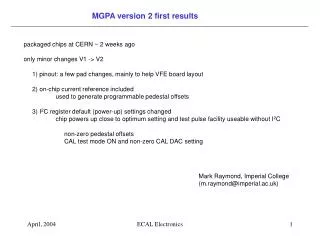
MGPA version 2 first results packaged chips at CERN ~ 2 weeks ago only minor changes V1 -> V2 1) pinout: a few pad changes, mainly to help VFE board layout 2) on-chip current reference included used to generate programmable pedestal offsets 3) I2C register default (power-up) settings changed chip powers up close to optimum setting and test pulse facility useable without I2C non-zero pedestal offsets CAL test mode ON and non-zero CAL DAC setting Mark Raymond, Imperial College (m.raymond@imperial.ac.uk) ECAL Electronics
On-chip current reference (1) measured pedestal dependence on supply voltage – VERSION 1 • this result presented Nov. 03 • big improvement in pedestal stability possible • if Iref to offset bias generator made constant • need supply independent current generator on chip ECAL Electronics
On-chip current reference (2) VERSION 2 on-chip current reference standard circuit (used before) Iref depends on Vth and R but not on supply voltage put circuit in corner of chip near BIAS_IIN pad scrap BIAS_ENB function (not used) and replace by BIAS_IOUT (link on PCB) Vth R BIAS_IOUT BIAS_ENB BIAS_IIN BIAS_IIN VDD VDD VDD VDD 79 78 77 76 79 78 77 76 75 75 V1 V2 ECAL Electronics
On-chip current reference (3) measured pedestal dependence on supply voltage – VERSION 2 Internal Iref high gain range: ~ flat response @ nominal 2.5 V at extremes of VDD range (2.375, 2.625) get 1 lsb pedestal drift for ~ 5mV VDD drift should be no problem for local regulators to achieve this in stable temperature environment VDD spec. (2.5V +/- 5%) ECAL Electronics
Changes to I2C default settings (1) zero pedestal offset 1)non-zero default settings for pedestals differential output signal naturally bias up to centre of range => need to apply offset at diff stage I/P to make full use of dynamic range programmable offset derived from current reference switch on (reset) value now defaults to 64 for MGPA V2 2) cal mode ON and non-zero DAC value allows use of test pulse without needing I2C to enable and program test pulse amplitude correct offset applied ECAL Electronics
Changes to I2C default settings (2) all 3 pedestal offset registers now default to 64 -> close to optimum (can still use I2C to fine tune) changes to defaults for test pulse settings also check out OK ECAL Electronics
Pulse shape comparison V1 vs. V2 MID HIGH LOW pedestals subtracted RAL test board modified (jumpers) so that either version can be plugged in -> identical performance, gain ratios identical -> note: absolute gain determined by on-chip resistors (+/- 10% tolerance) ECAL Electronics
Summary MGPA – V2 engineering run successful only significant electronic changes V1 -> V2 are: 1) on-chip current reference 2) changes to I2C default settings tests show both changes have worked (no change carries zero risk) basic performance measurements show identical behaviour to previous version ECAL Electronics