Advanced X-Ray Techniques in Industrial Applications for Thin Films
530 likes | 693 Vues
Explore industrial applications of X-ray reflectivity and thin films in electronics, materials, and energy sectors. Discover high-density interfacial layers and accurate analysis methods for ultra-thin films using advanced X-ray technology.

Advanced X-Ray Techniques in Industrial Applications for Thin Films
E N D
Presentation Transcript
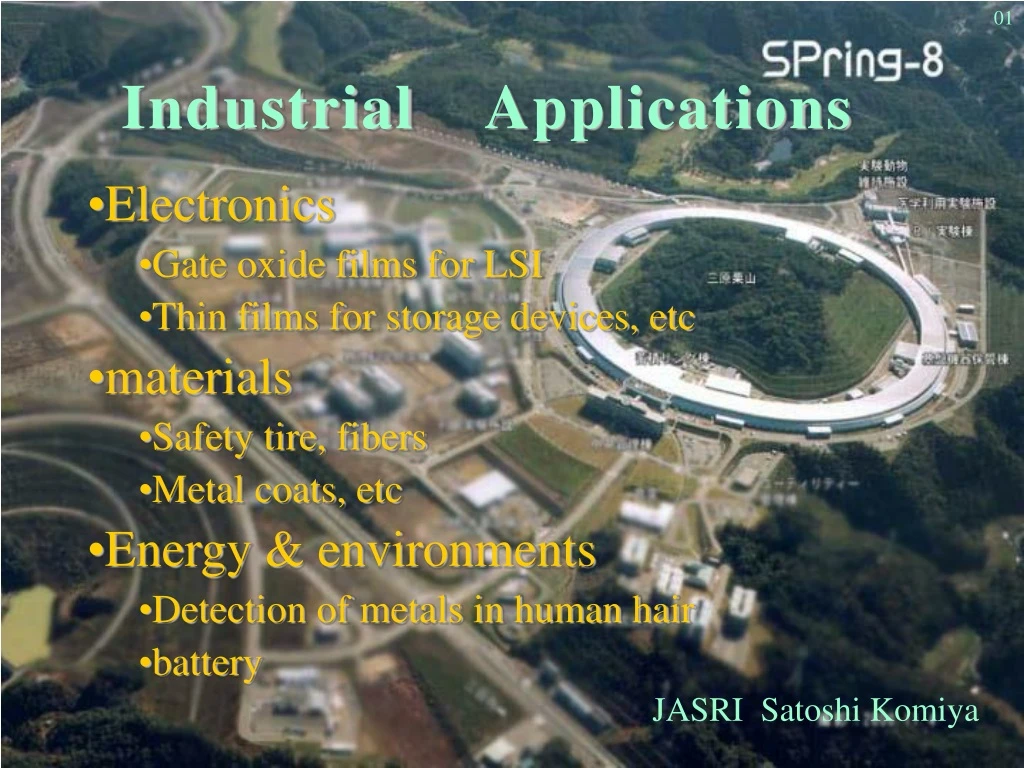
01 Industrial Applications • Electronics • Gate oxide films for LSI • Thin films for storage devices, etc • materials • Safety tire, fibers • Metal coats, etc • Energy & environments • Detection of metals in human hair • battery JASRI Satoshi Komiya
02 Industrial Applications of SR Characterization of materials • Structure, Chemical state, Contamination, etc. • thin films for electronic devices;LSI, HDD, lasers • metals、polymers, batteries,catalyses • high brilliant source, x-ray;big machine Production technology • lithography, photo-assisted etching or deposition • high flux source, ultra-violet-soft x-ray; • small machine
03 Industrial Applications • Films for ULSI, semiconductors • HDD, DVD • Semiconductor laser • Steel & Coats on steel • Al included bubbles • Tires • Fibers electronics Metals & Soft materials Synchrotron radiation Energy & Environment Life science Others • Building materials • Catalysis • Insects • Batteries: fuel cell & Li-ion • Analysis of contamination elements • Catalysts for environment • medicine
04 lines barrier metals Isolated oxides gate oxides silicide contacts CMOS Structure key points for R&D:gate & lines cross section
05 Detector θ‐ 2θ incident Reflection Diffraction Sample ψ‐ 2ψ Grazing incident x-ray reflection and diffraction High brilliant x-ray Structural analysis of thin films Incidence Reflection thin films Diffraction
06 100 reflection incidence 10-1 ψ ( 10-2 10-3 • Reflectivity Information • Period Thickness • Amplitude Density • Damping Roughness 10-4 10-5 10-6 10-7 TaOx/Si 10-8 10-9 0 1 2 3 4 5 6 X-ray reflectivity analysis Information obtained by reflectivity analysis Reflection Intensity Incidence angle(θ)
07 Bare Si SiO2 Native oxide Si substrate Reflection intensity Incidence Angle (deg) X-ray reflectivity profiles of oxide films on silicon substrates Accuracy Thickness:0.01nm Density:0.01g/cm3 Roughness:0.02nm
08 X-ray reflectivity profile and interference components (calculation) ρSiO2 > ρSi SiO2 on Si thickness:4nm ρSi=2.33 g/cm3 Interference components ΔR=log10(R/Rave) Rave:reference ρSiO2 < ρSi Subtraction technique of the interference component derive easy analysis.
09 Analysis with the interference component Single layer model Double layer model Interfacial layer 4nm thin SiO2 on Si fabricated by thermal oxidation
10 Generation of high dense interfacial layer on thermal oxidation process dry wet SiO2 Temperature(℃) Temperature(℃) Si Interfacial layer high dense, ~1nm thick N.Awaji et al., JJAP 35(1996)L67.
11 13 12 11 10 9 8 7 6 5 4 3 2 1 log10I (cps) 0 -1 0 5 10 15 20 25 30 35 40 45 50 2θ (deg) Development of measurement technique Accurate evaluation of ultra-thin films SiO2 1.0 nm Si(002) BL16XU Same region BL16B2 BL16XU:undulator beamline BL16B2:bending magnet beamline N.Awaji in Fujitsu Labs.
12 Si(111) Observation of crystalline SiO2 in thermal oxides a-SiO2 SiO2/Si 1.1nm crystalline SiO2 high dense interfacial layer Si Interference fringes X-ray Crystal Truncation Rod Scattering I.Takahashi et al., Physica B245(1998) 306.
13 1000 8hr 3.5hr 7hr 900℃ amorphous SiO2 3hr 6hr 5hr 2.5hr 4hr 2hr 1hr30min 1hr15min 1hr Thickness(nm) 30min 900℃ 15min Si RT Intensity(cps) 100 300C crystalline SiO2 300C after 900C 8hr growth of crystalline SiO2 at the interface at RT 0.3 0.35 0.4 0.45 0.5 0.55 0.6 0.65 0.7 (1,1,L) (Crystal Truncation Rod) Growth Time(hr) In-situ observation of CTR scattering during thermal oxidation interface layer = oxidation front : ~1 nm at RT fundamental phenomena on thermal oxidation N.Awaji Appl. Phys. Lett., 74(1999)2669.
14 Si3+ Si4+ Si2+ Si1+ Si O Analysis of Si-oxidation by XPS hν=130eV Si2p SiO2 (~0.6 nm) on Si(001)2x1 Polar emission angle : normal 0.14nm Transition layers Transition layer model 3rd Si3+/Si4+ (Si3+<<Si4+) 2nd Si3+/Si4+ (Si3+<Si4+) 1st Si1+/Si2+ (Si1+<Si2+ ) Photoelectric intensity (a.u.) Surface sensitive condition Polar emission angle : 60deg. Kinetic energy (eV) J.H. Oh et al., Phys. Rev. B63, 205310 (2001)
15 Hard Disk Drive Head MO Memory density (Mbit/in2) HDD year
16 X-ray reflectivity analysis of multi-layers Reflection intensity Incidence angle (deg) Y.Kitade in Fujitsu Labs.
17 PC Optics SR Analyzer LiF, PET SC/PC Soller slit PC fluorescence Reflected x-ray Incident x-ray GMR multi-layers Wavelength dispersive X-ray fluorescence Optics Fluorescence spectra from spin-valve multi-layers with grazing incidence
18 ~ ~ ~ ~ ~ ~ ~ ~ ~ ~ X-ray fluorescence intensity (a.u.) 0.0 0.0 0.1 0.1 0.2 0.2 0.3 0.3 0.4 0.4 0.5 0.5 0.6 0.6 0.7 0.7 φ (deg) φ (deg) X-ray incident angle (deg) Grazing Incidence X-ray Fluorescence Technique X-ray fluorescence Cu Fe Ta Pt reflection incidence Standing wave is induced into multi-layers
19 1.0 As deposited 0.8 T.L. D.L. 0.6 Profile (Normalized) Cu CoFeB PdPtMn NiFe CoFeB Ta Ta Si TaOx 0.4 0.2 0.0 -100 0 100 200 300 400 500 T.L. 1.0 390℃ annealed 0.8 D.L. 0.6 NiFe Ta Profile (Normalized) Si Cu CoFeB CoFeB PdPtMn Ta TaOx 0.4 0.2 0.0 -100 0 100 200 300 400 500 t(Å) Broadening of the interfaces in GMR multilayers 3Å 5Å 8Å 4Å 7Å 13Å (magnetic properties degraded after annealing) Depth profiles of elements analyzed from GIXF and reflectivity data N.Awaji Fujitsu scientific & technical journal 38 (2002) 82.
20 5~20nm 5~30nm 5~50nm NiP record along a circle and in-plane magnetization texture magnetization along a circle along a radius a-C cover layer Co alloy recording layer Cr buffer layer along a circle Al substrate diffraction hard disk cross section a coercive force B Hc c:magnetization axis control the orientation H circular Co alloy : hcp crystal radial
21 7 3 Co(002) 6 5 2 4 Intensity (a. u.) Co(101) Co(100) 3 1 2 1 0 0 25 30 35 40 25 30 35 40 Grazing incidence x-ray diffraction profiles Textured-Al/NiP/Cr/Co-alloy(20nm)/a-C Co(002) Cr(110) preferential orientation of c-axis due to texture along a circle from Cr buffer layer Intensity (a. u.) Cr(200) ψ=0.5° Co(002) from only a Co layer under grazing incidence circle Co(101) Co(100) radius ψ=0.2° 2θ (deg) 2θ (deg)
22 :along a circle :along a radius 2000 1500 Coercivity Hc(Oe) 1000 500 0 2 4 6 8 10 Intensity ratio I[Co(002)]/I[Co(100)] Preferential c-axis orientation dependence of coercive magnetic force Textured sub.(Ra50) Increase in coercive force due to preferential c-axis orientation along a circle T.Hirose IEEE Trans. Mag. 33. (1997) 2971.
23 InN-composition (%) 10 20 35 400 470 520 Emission wavelength(nm) Blue laser for DVD optical storage devices Red: GaAlAs Blue: Ga1-xInxN How is local structure in GaInN with low In composition less than 20% which is the critical composition for the phase separation?
24 InN composition dependence of GaInN XAFS
25 InN composition dependence of radial distribution functions wurtzite crystal structure (a=3.189Å, c=5.185Å for GaN) Monotonic decrease in the second peaks from In-Ga(In)
26 N Ga In InN composition dependence of the local structure Change of bond angles InN composition dependence of atomic distances
27 Deviation from random distribution of Ga and In atoms in GaInN mixed crystal In composition dependence of the 2nd neighbor coordination numbers T. Miyajima phys. Stat. Sol. (b) 228, 45 (2001).
28 Record&elimination by laser exposure • High power→amorphous formation by quenching • Low power→crystallization by annealing Phase transition storage materials for DVD ーAccurate structure analysis with a Debye-Scherrer cameraー Recorded mark Phase transition materials • AuGeSnTe • GeSbTe • AgInSbTe Debye-Scherrer camera What materials are excellent in high speed record/elimination and reliability
29 (+) experiments calculation difference X-ray power diffraction with SR Ag3.4In3.7Sb76.4Te16.5 With a laboratory source Excellent resolution X-ray powder diffraction with SR source
30 Fine crystalline structure of AgInSbTe Ag3.4In3.7Sb76.4Te16.5 At low temperature At high temperature Temperature dependence of lattice parameteres • Random occupancy of Ag, In, Sb, Te • Simple cubic units R32/R3m T. Matsunaga Phys. Rev. B64 (2001)184116.
31 Common properties on three materials z z z y y x x y x GeTe-Sb2Te3Au25Ge4Sn11Te60Ag3.4In3.7Sb76.4Te16.5 • Unique crystalline phase • Poor package :simple cubic, allowance of many vacancies • Random occupancy of component atoms at lattice sites
32 Modulator region DFB-LD region Development of laser diodes for optical communications A package process for fabrication of lasers with various wavelength DFB laser diode integrated with wave length modulator for WDM optical communications system Control of wave length Narrow-strip selective metal-organic vapor phase epitaxy (MOVPE)
33 X-ray micro-beam Formation of x-ray micro-beam with asymmetric diffraction 数μm
34 14 10 13 10 m W = 0 m 12 m 10 0.75 11 10 m = 4 m 10 10 m = 6 m 0.70 9 10 m = 8 m 8 10 m = 10 m 7 0.65 10 m = 15 m 6 10 m = 20 m 5 10 0.60 m = 25 m 4 10 m = 30 m 3 10 0.55 m = 40 m 0 10 20 30 40 2 10 -10 0 10 20 30 -3 D ´ q / q ( 10 ) Determination of process condition S.Kimura et al., APL 77(2000) 1286. In composition (x) As composition (y) Composition (x,y) Intensity InxGa1-xAsyP1-x Mask width (μm) Mask width dependence of lattice parameter Mask width dependence of composition (x,y) 40% up on emission efficiency of semiconductor laser
35 Detector (SSD) Incident X-ray Reflected X-ray Sample (Si wafer) NiKα CoK α EDX WDX Intensity(arbitrary unit) CoK β FeK β 6.5 7 7.5 8 E(keV) X-ray fluorescence analysis PC SSD Optics Energy dispersive (EDX) SR • High sensitivity • Low energy resolution Wave dispersive (WDX) Analyzing crystals: LiF(200), PET(002), multi-layers Detectors (SC, FPC) Solar slit • low sensitivity • high energy resolution Incident X-ray Reflected X-ray Sample (Si wafer)
36 HF drop Bare Si surface EDX WDX Native oxide HF drop dissolve native oxide automatically. After concentration To the center Dry Before concentration Concentration of contamination atoms Ultra-low detection limit M. Takemura in TOSHIBA ITRS road map atoms/cm2 4x10⁶ atoms/cm2 = 4 atoms/100μm2
37 Direct observation of fibers in safety tire press SEM image tire fiber Sharp edge image ice Refractive contrast image Fibers stick into ice SR source Direct observation of fibers sticking into ice Difference of absorption X-ray tube R&D on safety tire on ice
38 tire fibers space ice Fibers slip from ice press pull Fibers stick into ice tire tire ice ice H. Kishimoto in Sumitomo Rubber Industries
39 Press Observation of crush of babbles in Al T. Watanabe in Kobelco Research Institute CCD X-ray Shock absorber for crush Images stored during 2 sec 1mm Crush from the bottom side Crush from the both sides Crush all
40 Light guide Zn Fe-Zn alloy IR heater IR Melt & Alloy Fe (base) Quartz holder Sample chamber 試料 slit slit detector Ion chamber 2° 2θ Holder (quartz) I Thermocouple I0 In-situ observation of alloying of galvanized steel by Zn Lamp heater Diffractmeter Rust preventive coat
41 1.4 1.2 1.0 0.8 Normalized Peak Area 0.6 0.4 0.2 0.0 0 50 100 150 200 Time / s Alloying process of Zn on steel 480℃ FeZn10(δ1) Amount of δ1 crystals ∝ √t (integrated intensities) ⇒Controlled by diffusion process Zn-0.14mass%Al Variation of diffraction profiles on alloying A. Taniyama SPring-8 User Experiment Report 2002A0658.
42 240μm) ZrO2 NiCoCrAlY Characterization of inner stress in coats on turbine blades Ni3Al(311) furnace Diffractometer Coat to protect blades from high temperature gas Variation of diffraction profiles on heating Gas turbine K. Suzuki SPring-8 User Experiment Report No.8 2001B0063.
43 ○Tc=0.24mm ●Tc=0.083mm 2θdeg. Diffraction angle Softening Residual stress (MPa) tensile sin2ψ compressive Temperature (K) Temperature dependence of residual stress in bond-coat Tc=0.24mm 2θψ∝constant – Kσsin2ψ K=(tanθ0)2(1+ν)/E ν:Poisson’s ratio E:Young’s modulaus Z ψ Surface normal Diffract plane nomal Temperature dependence of residual stress in bond-coat
44 X-ray micro-beam with zone plate Focus with zone plate ~μm
45 A single fiber X-ray Strain of crystal (%) weighting Stress [MPa] Structural analysis of a single fiber Stress-strain of a PBO single fiber 0.01mm in diameter Structural change at local parts in complex fibers M.Kodera in JASRI
46 Cu Zn 1.4 40 1.2 1.0 30 0.8 20 0.6 0.4 10 0.2 125 0 0 Cu in human hear fg ppm 100 75 Y (μm) 50 25 10-40 ppm 0 0 25 50 75 100 125 X (μm) 2-D mapping of a very small amount of metals with x-ray fluorescence analysis (1 fg = 10-15 g) Influence of special water from deep sea on the body Y.Kagoshima Nucl. Instrum. & Methods. A 467-468(2001) 872.
47 Capacity fading on Li ion battery during charge/discharge cycles ーIn-situ XAFS study on cathode during cycling of batteryー X-ray Cathode:LiNi0.8Co0.2O2 Coin cell Coin cell Ni K-edge XANES spectra of LiNi0.8Co0.2O2
48 Decrease in capacity due to no return of Li into cathode capacity capacity O Ni Li+ NiO6
49 O Ni Mechanism of the capacity fading Jahn-Teller distortion Li+ Initial:distorted NiO6 octahedron After fading:regular NiO6 octahedron NiO6 T.Nonaka J. Synchrotron rad., 8 (2001) 869.
50 Request to analysis on material science in industry • No detectable with other techniques • How situation : Research, Development, Production • R&D:Excellent characterization • Development of process : regular measurement according to plan • Test:Quality & Quantity & Time • Response to trouble : Speed How can we (SR) reply on request?